
Switch circuit and method of switching radio frequency signals

Active Publication Date: 2009-11-03
PSEMI CORP
View PDF34 Cites 19 Cited by
  • Summary
  • Abstract
  • Description
  • Claims
  • Application Information

AI Technical Summary

Benefits of technology

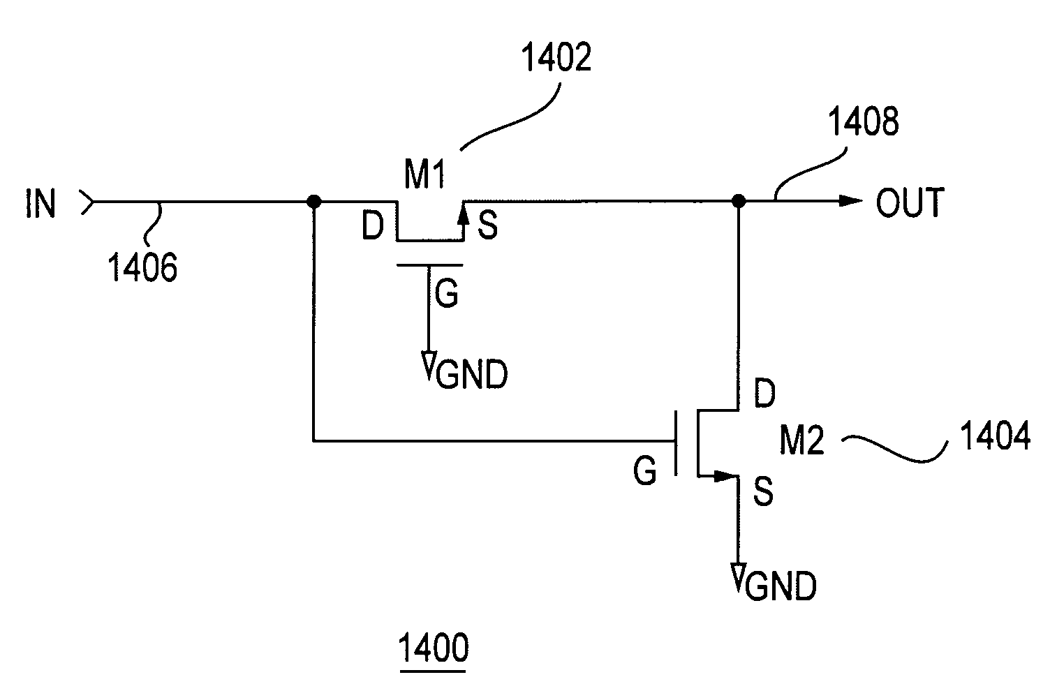
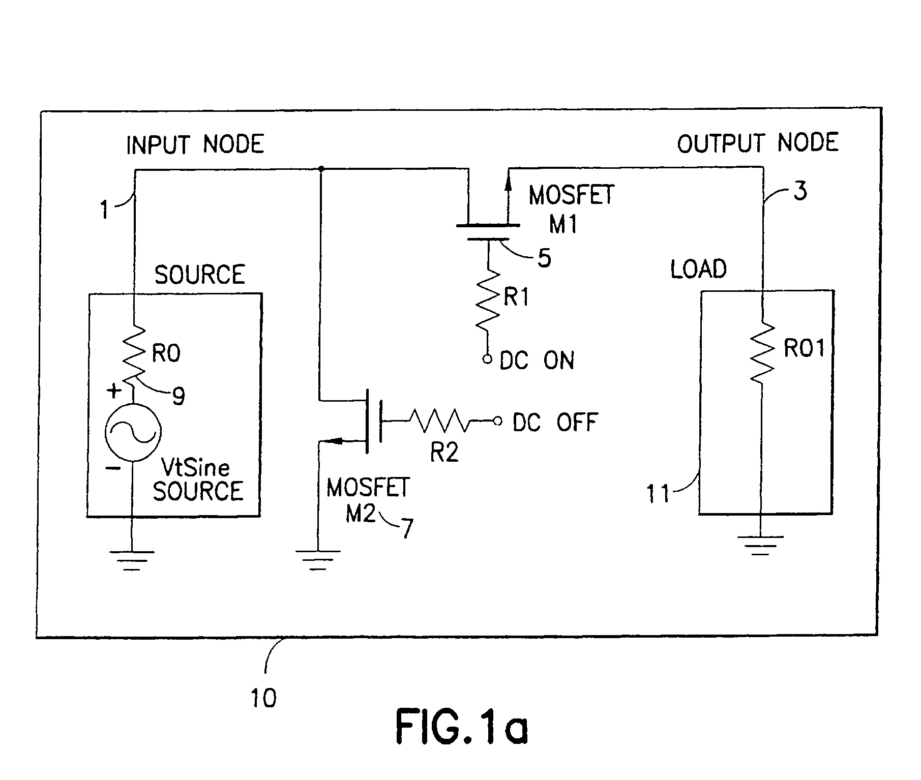
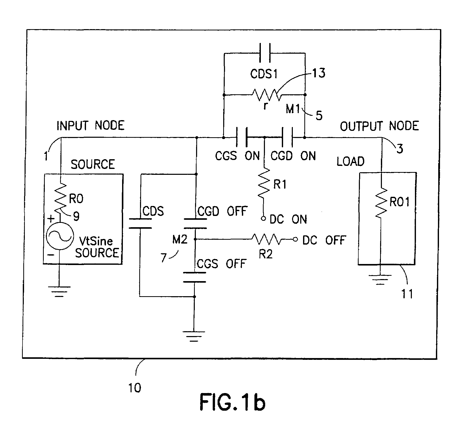
[0021]A novel RF switch circuit and method for switching RF signals is described. The RF switch circuit may be used in wireless applications, and may be fabricated in a silicon-on-insulator technology. In one embodiment the RF switch is fabricated on an Ultra-Thin-Silicon (“UTSi”) substrate. In one embodiment the RF switch includes: an input for receiving an RF signal; a first switching transistor grouping connected to the input to receive the RF signal and connected to an RF common port, wherein the first switching transistor is controlled by a switching voltage (SW); a second switching transistor grouping connected to the first switching transistor grouping and the RF common port, wherein the second switching transistor is controlled by a switching voltage SW_, and wherein SW_ is the inverse of SW so that when the first switching transistor grouping is on, the second switching transistor grouping is off. The switching transistor groupings, when enabled, alternatively connect their respective RF input signals to the RF common port. In this embodiment the RF switch also includes shunting transistor groupings coupled to the switching transistor groupings and also controlled by the switching voltages SW and SW_. The shunting transistor groupings, when enabled, act to alternatively shunt their associated RF input nodes to ground thereby improving RF switch isolation.
[0023]A fully integrated RF switch is described that includes digital switch control logic and a negative power supply voltage generator circuit integrated together with the RF switch. In one embodiment, the fully integrated RF switch provides several functions not present in prior art RF switches. For example, in one embodiment, the fully integrated RF switch includes a built-in oscillator that provides clocking input signals to a charge pump circuit, an integrated charge pump circuit that generates the negative power supply voltages required by the other RF switch circuits, CMOS logic circuitry that generates control signals to control the RF switch transistors, level-shifting and low current voltage divider circuits that provide increased reliability of the switch devices, and an RF buffer circuit that isolates RF signal energy from the charge pump and digital control logic circuits. Several embodiments of the charge pump, level shifting, voltage divider, and RF buffer circuits are described. The RF switch provides improvements in insertion loss, switch isolation, and switch compression. In addition, owing to the higher levels of integration made available by the present RF switch, RF system design and fabrication costs are reduced and reliability is increased using the present teachings.

Problems solved by technology

Feedthrough of the input signal is undesirable and is directly related to the input-to-output isolation of the RF switch 10.
This loss of power increases for increased input power (i.e., input signals of increased power), and thereby causes a first type of compression.
At breakdown, the shunt device begins to heavily conduct current thereby reducing the power available at the output.
The prior art RF switch implementations attempt to improve the RF switch performance characteristics described above, however, they do so with mixed results and with varying degrees of integrated circuit complexity and yields.
For example, bulk CMOS RF switches disadvantageously exhibit high insertion loss, low compression, and poor linearity performance characteristics.
For example, GaAs technology exhibits relatively low yields of properly functioning integrated circuits.
GaAs RF switches tend to be relatively expensive to design and manufacture.
In addition, although GaAs switches exhibit improved insertion loss characteristics as described above, they may have low frequency limitations due to slow states present in the GaAs substrate.
The technology also does not lend itself to high levels of integration, which requires that digital control circuitry associated with the RF switch be implemented “off chip” from the switch.
The low power control circuitry associated with the switch has proven difficult to integrate.
This is disadvantageous as it both increases the overall system cost or manufacture, size and complexity, as well as reducing system throughput speeds.
Such integration has been heretofore difficult to achieve using Si and GaAs substrates.

Method used


Image

  • Switch circuit and method of switching radio frequency signals
  • Switch circuit and method of switching radio frequency signals
  • Switch circuit and method of switching radio frequency signals

Examples


first embodiment

A First Embodiment

[0077]As shown in FIG. 4, one embodiment of the fully integrated RF switch 100 includes a negative voltage generator or charge pump 120. The negative voltage generator 120 generates the negative power supply voltage (specified hereafter as “−Vdd”) required by other circuits of the fully integrated RF switch 100. Two sets of inputs are provided to the negative voltage generator 120: a positive DC power supply voltage signal (Vdd) 122; and a clocking input (shown in the figure as a single input signal, “Clk”) 124. Although the clocking input 124 is shown as a single input signal in FIG. 4, as described below with reference to FIG. 5b, in some embodiments of the RF switch, the clocking input 124 may comprise two or more clock input signals.

[0078]In addition, in the embodiment shown in FIG. 4, the positive supply voltage that is input to the negative voltage generator circuit 120 comprises a 3 VDC power supply. However, other power supply levels may be used without dep...

improved embodiment

[0127]As described above with reference to FIGS. 9a, 9b, and 10, it is sometimes desirable to limit the voltage levels applied to certain selected nodes within an electronic circuit in order to prevent excessive voltage swings from detrimentally affecting performance and reliability of the circuit. For example, as described above, unless a voltage reduction circuit is employed, voltage levels of 2*Vdd can be applied across the gate oxides of the feedback inverters 304, 310 of the level shifter 300 (see FIG. 6a). For example, in one embodiment where Vdd=+3V, and −Vdd (or “Vss”)=negative 3V, a gate-to-source voltage (Vgs) of 6 Volts can be applied to the gate oxides of the feedback inverters 304, 310. As described above, such excessive voltages can detrimentally affect both the performance and reliability of the level shifter 300, and can eventually irreparably harm the feedback inverters 304, 310. Therefore, as described above with reference to the first exemplary embodiment of the v...


PUM


Abstract

A novel RF switch circuit and method for switching RF signals is described. The RF switch circuit is fabricated in a silicon-on-insulator (SOI) technology. The RF switch includes pairs of switching and shunting transistor groupings used to alternatively couple RF input signals to a common RF node. A fully integrated RF switch is described including digital control logic and a negative voltage generator integrated together with the RF switch elements. In one embodiment, the fully integrated RF switch includes a built-in oscillator, a charge pump circuit, CMOS logic circuitry, level-shifting and voltage divider circuits, and an RF buffer circuit. Several embodiments of the charge pump, level shifting, voltage divider, and RF buffer circuits are described. The RF switch provides improvements in insertion loss, switch isolation, and switch compression. An improved voltage reducing circuit is described. The improved voltage reducing circuit limits voltages applied to selected nodes within the integrated circuit.

Description

CROSS-REFERENCE TO RELATED APPLICATIONS—CLAIMS OF PRIORITY[0001]This application claims a benefit of priority under 35 U.S.C. § 119 (e) to U.S. Provisional Application No. 60 / 571,220, filed May 14, 2004, entitled “Improved Switch Circuit and Method of Switching Radio Frequency Signals”. Co-pending and commonly assigned application Ser. Nos. 10 / 922,135 (subsequently issued Oct. 17, 2006 as U.S. Pat. No. 7,123,898), provisional application 60 / 571,220, and commonly assigned U.S. Pat. No. 6,804,502, and its related Provisional Application No. 60 / 328,353, filed Oct. 10, 2001, are all hereby incorporated by reference herein in their entireties for their background teaching in respect of RF Switch design and manufacturing.BACKGROUND[0002]1. Field[0003]The present disclosure relates to switches, and particularly to a switch circuit and method of switching radio frequency (RF) signals within an integrated circuit. In one embodiment, the switch circuit comprises CMOS devices implemented on a ...

Claims


Application Information

Patent Timeline
IPC IPC(8): H04B1/28H01L29/76H04M1/00
CPCH03K17/693H03K17/063
Inventor KELLY, DYLAN J.BURGENER, MARK L.CABLE, JAMES S.
Owner PSEMI CORP
Learn More