Apparatus for measuring waveform of optical electric field, optical transmission apparatus connected thereto and a method for producing the optical transmission apparatus

a technology of optical electric field and optical transmission apparatus, which is applied in the direction of electromagnetic transmission, optical radiation measurement, instruments, etc., can solve the problems of low measurement precision, large phase measurement error, and inability to measure the value of optical phase, so as to improve measurement accuracy, remove noise components, and improve measurement accuracy

Inactive Publication Date: 2009-11-10
HITACHI LTD
View PDF2 Cites 8 Cited by
  • Summary
  • Abstract
  • Description
  • Claims
  • Application Information

AI Technical Summary

Benefits of technology

[0022]It is therefore an object of the present invention to provide a simple method of observing an optical electric field waveform with higher precision and higher time resolution, the method being applicable to any high-speed modulation optical signal such as a phase modulation signal and a conventional intensity modulation signal.
[0037]In the assembly process of the optical transmitter, by employing a process in which while measuring the optical electric field waveform by the optical electric field waveform measuring apparatus of the present invention, the waveform is adjusted to an ideal state; there is attained an advantage that the waveform distortion of the optical transmitter is reduced and the transmission characteristics such as the receiving sensitivity is improved.

Problems solved by technology

This leads to a problem that the absolute value of the optical phase cannot be measured and a problem that the measurement is accompanied by quite a large phase measurement error.
It is hence likely that the measurement precision lowers due to the limit of the time resolution and the restriction of the frequency band of the measuring apparatus.
Also, the linear measurement range of the apparatus can be easily exceeded to cause a measurement error.
Contrarily, in a case in which the phase variation slowly occurs through at least several bits, there exists a problem that the frequency chirp is too small to be appropriately measured.
Therefore, it is not possible to use the frequency chirp measuring apparatus for the evaluation of the inter-symbol interference of such signals.
On the other hand, the conventional phase observing method represented by the digital phase diversity method is accompanied by problems as below.
The first problem resides in the difficulty in the evaluation of the inter-symbol interference (transmission waveform distortion) of the optical electric field waveform.
However, the received waveform after the detection includes waveform distortion and hence is not suitably used to evaluate the transmitted waveform.
The method of independently observing the eye pattern of the in-phase and quadrature components is unable to completely obtain the variation in the optical electric field and is hence not suitable for the evaluation of an optical signal such as the QPSK signal in which the in-phase and quadrature components are simultaneously modulated.
There also exists a problem that the phase detection sensitivity is zero in the vicinity of a position where the in-phase component takes the minimum amplitude or the maximum amplitude and hence the phase rotation quantity of the optical signal cannot be evaluated.

Method used


Image

  • Apparatus for measuring waveform of optical electric field, optical transmission apparatus connected thereto and a method for producing the optical transmission apparatus
  • Apparatus for measuring waveform of optical electric field, optical transmission apparatus connected thereto and a method for producing the optical transmission apparatus
  • Apparatus for measuring waveform of optical electric field, optical transmission apparatus connected thereto and a method for producing the optical transmission apparatus

Examples


first embodiment

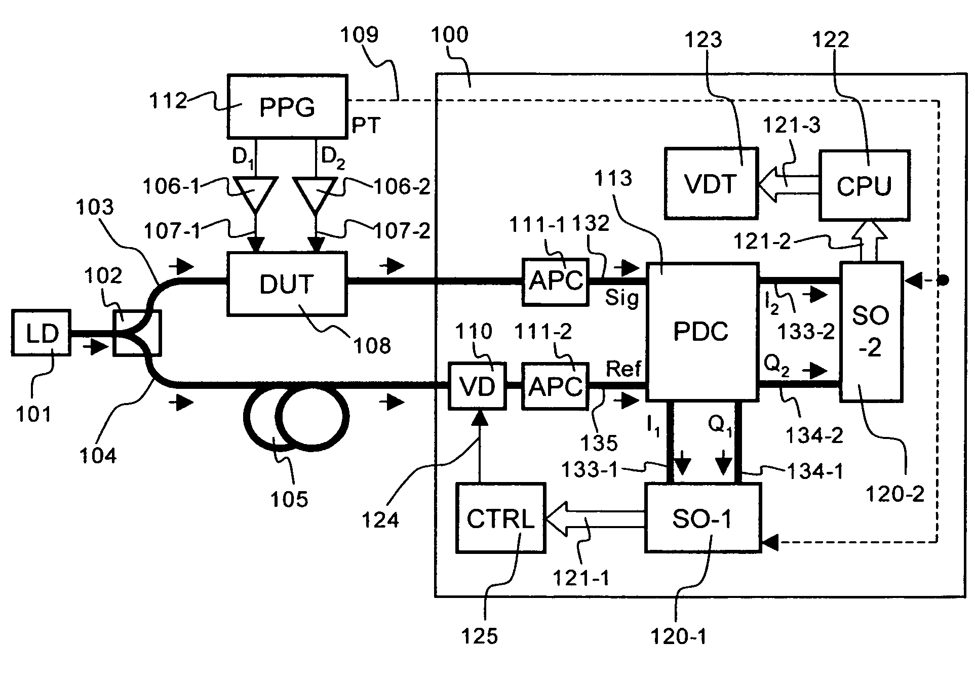
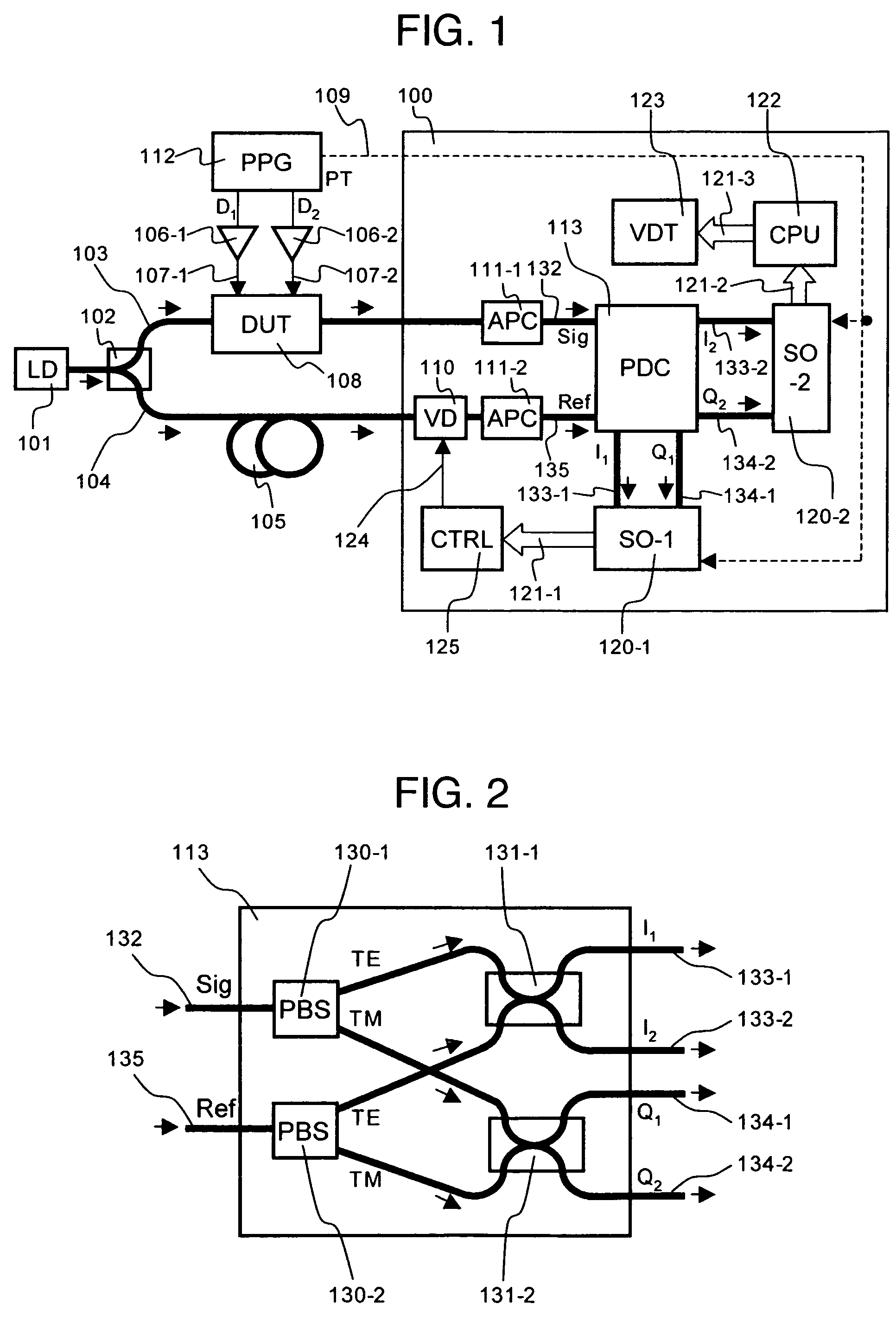
[0072]FIG. 1 shows the first embodiment of the present invention in a configuration diagram, showing a configuration example of an optical waveform observing apparatus according to the present invention. A laser beam emitted from the laser source 101 is divided by an optical coupler 102 into a first portion and a second portion to be fed respectively to an optical fiber 103 for signal light constituting a signal light path and an optical fiber 104 for reference light constituting a reference light path. The first portion passes through an optical modulator 108 to generate an optical signal as a measurement object and is fed to an optical waveform observing apparatus 100. The input signal passes through an automatic polarization controller 111-1 and is then delivered to a signal light input port 132 of an optical phase diversity circuit 113.

[0073]On the other hand, the second portion of the laser beam passes through an optical fiber delay line 105, a variable optical phase shifter 11...

second embodiment

[0094]FIG. 10 shows a configuration of the second embodiment of the present invention. This is an example in which the waveform measuring apparatus 100 includes the laser source 101 and the optical coupler 102. The waveform measuring apparatus of the present invention may be configured such that part of the constituent components are externally arranged or internally disposed in the apparatus according to necessity.

[0095]Also, in this example, the optical fiber delay line 105 of FIG. 1 is replaced with a variable optical delay circuit 150 and only one optical input sampling oscilloscope is employed to observe the optical signal. The delay circuit 150 includes optical switches 151-1 and 151-2 to change a path of the optical signal, fixed optical fiber delay lines 152-1 to 152-4 to delay the optical signal for a predetermined period of time, and an optical coupler 153 to synthesize optical signal paths into one path. In the example, the delay lines 152-1 to 152-4 have respectively len...

third embodiment

[0098]FIG. 11 shows a configuration of the third embodiment of the present invention. The example includes a homodyne interferometer configuration in which local emission is employed in place of the self-homodyne optical interferometer and the waveform observing apparatus 100 is configured using the digital phase diversity method. The interference method using such local emission source is advantageous in that the measurement of the optical electric field waveform is possible for an integrated light source including an external modulator and a laser source and for the optical waveform including phase deviation after transmission through the optical fiber for which delay adjustment is difficult. In the conventional digital phase diversity method described above, there exists a problem as follows. It is not possible to conduct the waveform observation with high precision and with high time resolution. Moreover, there does not exist the phase reference of the waveform and hence the lon...


PUM


Abstract

An electric field waveform of an optical signal is precisely measured with high time resolution. Particularly, determination of inter-symbol interference has been difficult. Output light from the laser source is divided into first and second portions. The first portion is modulated by an optical modulator. The second portion is delayed by a delay line for the same quantity of delay as that of the first portion. The first and second portions are fed to a phase diversity circuit to configure a homodyne interferometer. An optical input sampling oscilloscope stabilizes a variable optical phase shifter to set an optical phase at a particular point of time to a fixed value using a pattern sync signal as a reference. An optical input sampling oscilloscope repeatedly averages optical waveforms and a CPU conducts three-dimensional display of the optical electric field waveform from which noise has been removed.

Description

INCORPORATION BY REFERENCE[0001]The present application claims priority from Japanese application JP2005-252978 filed on Sep. 1, 2005, the content of which is hereby incorporated by reference into this application.BACKGROUND OF THE INVENTION[0002]The present invention relates to evaluation and measurement of an optical waveform employed for high-speed optical fiber transmission.[0003]In the existing optical fiber transmission to transmit information, optical signals are modulated according to intensity thereof into binary values, i.e., on and off. The optical signal modulation speed is rapidly increasing from 2.5 gigabits per second (Gbits / s) to 10 Gbits / s and then to 40 Gbits / s. The transmission distance of the optical fiber transmission is restricted by the wavelength dispersion of the optical fiber used for the optical transmission. It is known that the distance theoretically lessens in inverse proportion to the square of the bit rate. At a bit rate of 2.5 Gbits / s, the maximum tr...

Claims


Application Information

Patent Timeline
Patent Type & Authority Patents(United States)
IPC IPC(8): G01B9/02G01J11/00H04B10/07H04B10/079H04B10/25H04B10/524H04B10/54H04B10/556H04B10/58
CPCG01J11/00G01J9/02
Inventor KIKUCHI, NOBUHIKO
Owner HITACHI LTD
Why Eureka
Try Eureka