
Field effect transistor and method for manufacturing same

a field effect transistor and field effect technology, applied in the field of misfet, can solve the problems of increasing channel resistance, difficult to realize high-performance devices, and difficult to grow high-quality aln crystals on the surface of sic, and achieve the effect of leakage curren

Inactive Publication Date: 2009-11-24
JAPAN SCI & TECH CORP
View PDF7 Cites 12 Cited by
  • Summary
  • Abstract
  • Description
  • Claims
  • Application Information

AI Technical Summary

Benefits of technology

The invention provides a high-performance, insulated-gate SiC-based MISFET with a good interface with SiC and a high current-suppressing effect. By using an interface control layer and an insulating layer with a larger band offset with respect to a conduction carrier than the interface control layer, leakage current can be suppressed while a good interface condition is maintained. The invention also provides a method for manufacturing the field effect transistor with a simplified manufacturing process.

Problems solved by technology

However, when a metal-silicon oxide film-semiconductor field effect transistor (MOSFET), which is the basic structure of field effect transistor devices having an insulated gate, is prepared using SiC, the effective channel electron mobility at the SiO2 / SiC interface becomes much smaller than the electron mobility of bulk SiC, resulting in an increase in channel resistance.
As a result, the on-characteristics of the transistor deteriorate, making the realization of high-performance devices difficult.
However, it has been very difficult to grow a high-quality AlN crystal on the surface of SiC.
Because the only AlN layer that has been available was of low quality, a large leakage current flows in the AlN layer.
As a result, the AlN / SiC-based MISFETs that have been made have very poor gate insulating property in particular, and no devices have been realized that are suitable for practical application.

Method used


Image

  • Field effect transistor and method for manufacturing same
  • Field effect transistor and method for manufacturing same
  • Field effect transistor and method for manufacturing same

Examples


second embodiment

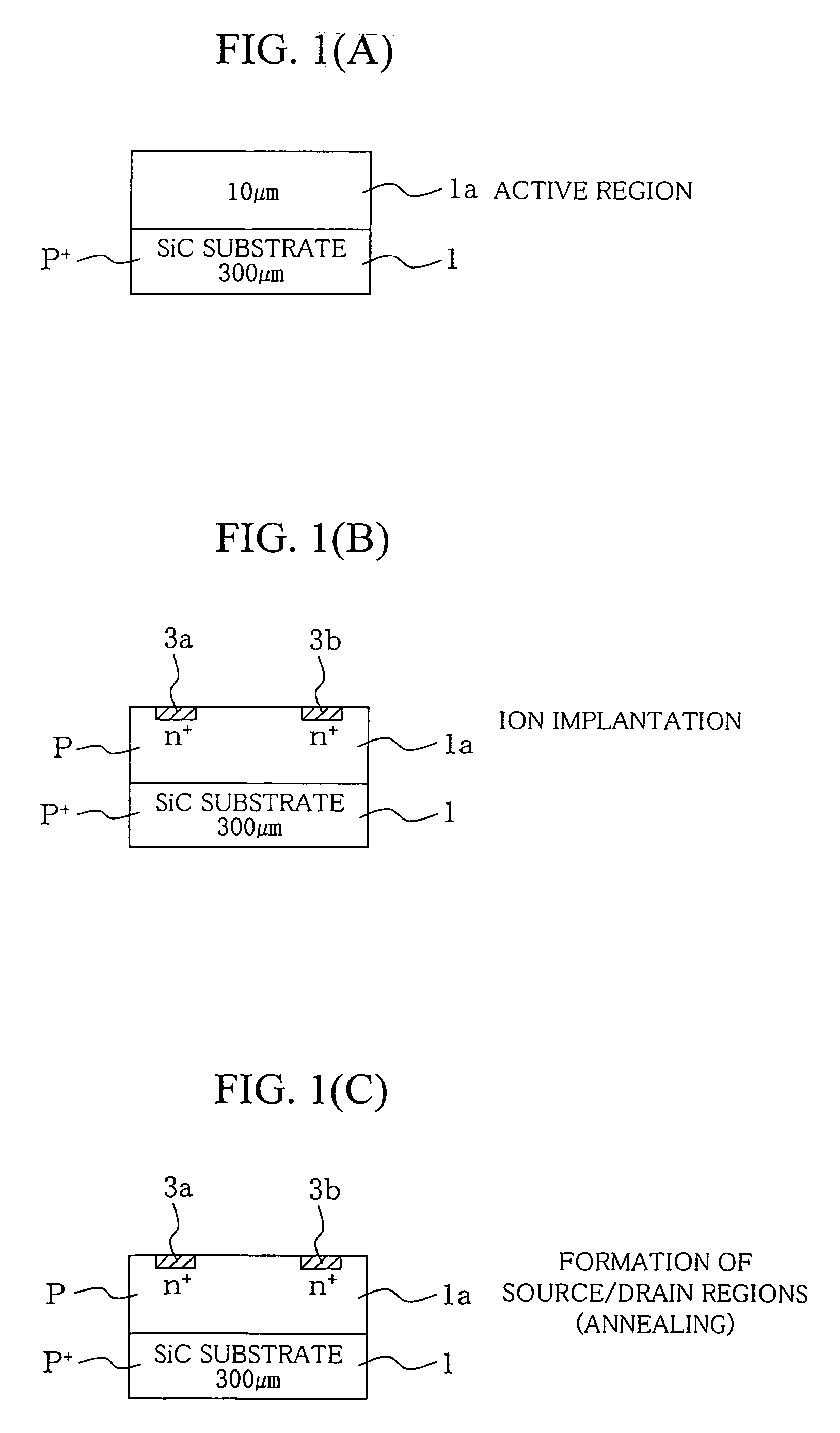
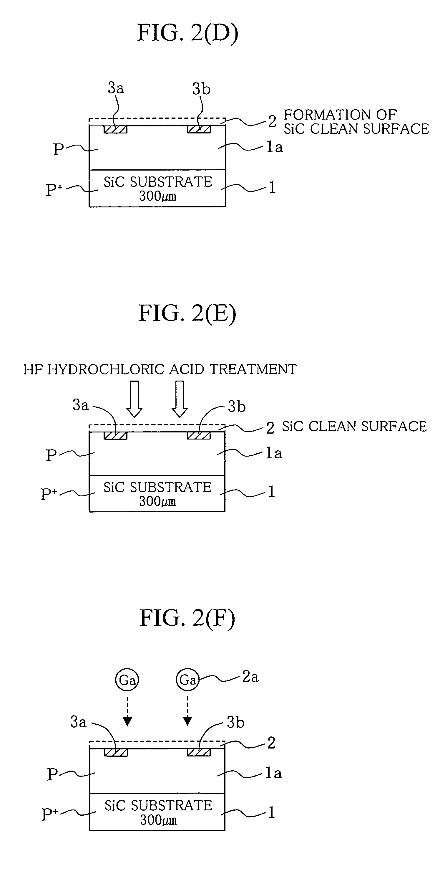
[0035]In the following, a MISFET according to the invention is described with reference to the drawings.

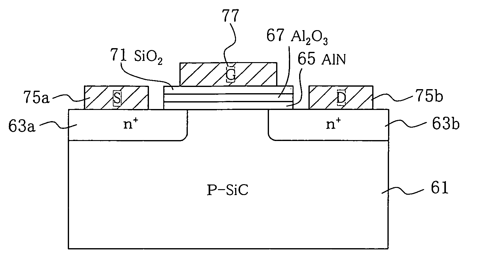
[0036]In the present embodiment, Al2O3 is used as the insulator on the gate electrode side. As shown in FIG. 5(A), the MISFET of the present embodiment includes source and drain regions 43a and 43b in a p-type SiC substrate 41 that are heavily doped with n-type impurities, layered structures 45 and 51 of AlN layer / Al2O3 layer formed between the source region 43a and the drain region 43b on the SiC substrate 1, and a gate electrode 55 formed on the layered structures 45 and 51. When the affinity with the AlN layer 45 is taken into consideration, it is preferable to use an insulator that contains Al as a component. In addition, Al2O3 is suitable for application in MISFETs because of its large bandgap, high insulation property, and large dielectric constant. FIG. 5(B) shows schematically the energy band structure of the SiC MISFET shown in FIG. 5(A) in the direction from the gate ele...

first embodiment

[0038]Thus, in accordance with the SiC-based MISFET of the present embodiment, the same effects as those obtained in the SiC-based MISFET can be obtained and, in addition, the manufacturing process can be simplified.

third embodiment

[0039]In the following, a SiC-based MISFET according to the invention is described with reference to the drawings. FIG. 7 shows a cross section of an example of the SiC-based MISFET of the present embodiment. As shown in FIG. 7, the SiC-based MISFET of the embodiment includes a source region 23a and a drain region 23b formed in a p-SiC substrate 21, a source electrode 31a and a drain electrode 31b formed on the source region and the drain region, respectively, a BxAl1-x-yGayN layer (x35. When a BAlGaN mixed crystal is used, the in-plane lattice constant can be substantially completely matched with SiC. If the lattice constants can be matched, distortion in the interface can be reduced and the development of misfit dislocation therein can be suppressed, which is preferable. If the mixed-crystal composition increases, the so-called alloy scattering, which is based on the fluctuation in the microscopic composition of the mixed crystal, increases, which would lead to a reduction of the ...


PUM


Abstract

A field effect transistor comprises a SiC substrate 1, a source 3a and a drain 3b formed on the surface of the SiC substrate 1, an insulating structure comprising an AlN layer 5 formed in contact with the SiC surface and having a thickness of one molecule-layer or greater, and a SiO2 layer formed thereon, and a gate electrode 15 formed on the insulation structure. Leakage current can be controlled while the state of interface with SiC is maintained in a good condition.

Description

TECHNICAL FIELD[0001]The present invention relates to a SiC-based MISFET and particularly to a MISFET having an AlN-based insulating film.BACKGROUND ART[0002]SiC has excellent physical property values including the forbidden-band width of 3 eV or greater and the extremely high breakdown field intensity of 2.5 MV / cm or greater. Thus, it is gaining attention as a semiconductor material that can be used for realizing an ultralow-loss power transistor, a high-output, high-frequency transistor, or a field effect transistor having an extremely small gate length, all of which cannot be realized theoretically with the existing semiconductors, such as Si and GaAs.[0003]However, when a metal-silicon oxide film-semiconductor field effect transistor (MOSFET), which is the basic structure of field effect transistor devices having an insulated gate, is prepared using SiC, the effective channel electron mobility at the SiO2 / SiC interface becomes much smaller than the electron mobility of bulk SiC,...

Claims


Application Information

Patent Timeline
Patent Type & Authority Patents(United States)
IPC IPC(8): H01L29/792H01L21/04H01L21/28H01L29/24H01L29/51H01L29/78H10B69/00
CPCH01L21/049H01L21/28158H01L29/267H01L29/803H01L29/66068H01L29/78H01L29/7883H01L29/802H01L29/511H01L29/1608H01L29/2003H01L21/18
Inventor SUDA, JUNMATSUNAMI, HIROYUKI
Owner JAPAN SCI & TECH CORP
Learn More