

Nonvolatile semiconductor memory device
a semiconductor memory and non-volatile technology, applied in semiconductor devices, digital storage, instruments, etc., can solve the problems of information leakage, no leading-edge process can be used, and increase the cost of processing, so as to prevent the increase of the area of a memory element, the effect of reducing the amount of applied bias and increasing the erase speed
- Summary
- Abstract
- Description
- Claims
- Application Information
AI Technical Summary
Benefits of technology
Problems solved by technology
Method used
Image

Examples
embodiment 1
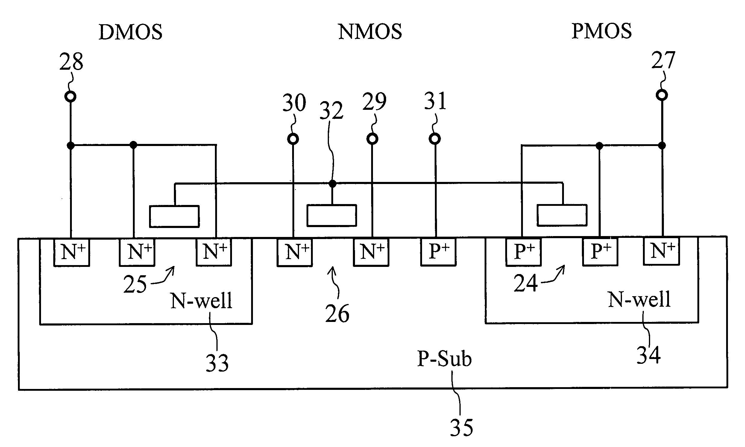
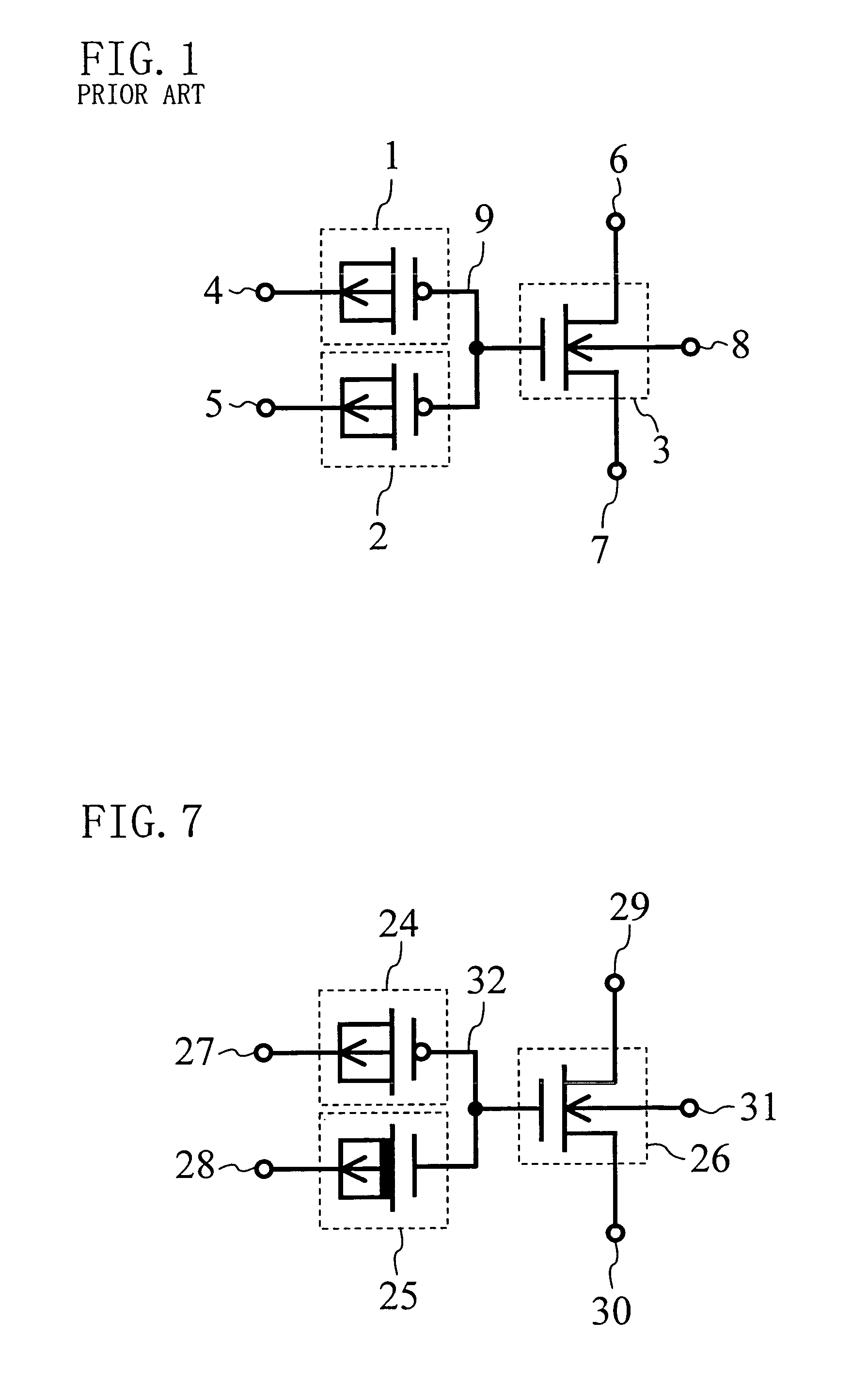
[0054]FIG. 7 is a circuit diagram illustrating a nonvolatile memory element according to a first embodiment of the present invention. FIG. 8 is a cross-sectional view of the nonvolatile memory element of the first embodiment. A nonvolatile memory element according to the present invention is constituted by three transistors: a control gate transistor 24 of a PMOS, a read transistor 26 of an NMOS and an erase gate transistor 25 of an n-type DMOS. The nonvolatile memory element of the present invention will be hereinafter referred to as a PMOS-NMOS-DMOS (PND) cell.
[0055]In FIG. 7, reference numeral 27 denotes a control gate (CG), reference numeral 28 denotes an erase gate (EG), reference numeral 29 denotes a drain terminal of the NMOS read transistor, reference numeral 30 denotes a source terminal of the NMOS read transistor, reference numeral 31 denotes a p-type silicon substrate terminal and reference numeral 32 denotes a floating gate (FG). In FIG. 8, reference numerals 33 and 34 d...
embodiment 2
[0059]FIG. 11 is a circuit diagram illustrating a nonvolatile semiconductor memory device having a differential cell structure according to a second embodiment of the present invention. One of the two parts forming a differential bit cell is referred to as a T (True) bit and the other is referred to as a B (Bar) bit. In FIG. 11, reference numeral 45 denotes a control gate transistor (a PMOS transistor) in the T bit, reference numeral 46 denotes an erase gate transistor (an n-type DMOS transistor) in the T bit, reference numeral 47 denotes a read transistor (an NMOS transistor) in the T bit, reference numeral 48 denotes a load PMOS transistor, reference numeral 49 denotes a control gate transistor (a PMOS transistor) in the B bit, reference numeral 50 denotes an erase gate transistor (an n-type DMOS transistor) in the B bit, reference numeral 51 denotes a read transistor (an NMOS transistor), reference numeral 52 denotes a load PMOS transistor, reference numeral 53 denotes a bit line...
embodiment 3
[0066]FIG. 15 is a circuit diagram illustrating a nonvolatile memory element according to a third embodiment of the present invention. In FIG. 15, reference numeral 89 denotes a program gate transistor (a PMOS transistor), reference numeral 90 denotes a control gate transistor (a PMOS transistor), reference numeral 91 denotes an erase gate transistor (a PMOS transistor), reference numeral 92 denotes a read transistor (an NMOS transistor), reference numeral 93 denotes a program gate (PG), reference numeral 94 denotes a control gate (CG), reference numeral 95 denotes an erase gate (EG), reference numeral 96 denotes a drain terminal of the NMOS read transistor, reference numeral 97 denotes a source terminal of the NMOS read transistor, reference numeral 98 denotes a p-type silicon substrate terminal and reference numeral 99 denotes a floating gate (FG).
[0067]FIG. 16 is a cross-sectional view of the nonvolatile memory element of the third embodiment. In FIG. 16, reference numerals 100, ...
PUM
 Abstract
Description
Claims
Application Information