

Circuits and design structures for monitoring NBTI (negative bias temperature instability) effect and/or PBTI (positive bias temperature instability) effect
a technology of circuits and design structures, applied in the field of electronic circuits, can solve the problems of significant reliability problems, reduced drive current for the device, and the degradation of the threshold voltage of the device in the presence of constant electrical and thermal stress, and achieve the effect of increasing the supply voltage and increasing the supply voltag
- Summary
- Abstract
- Description
- Claims
- Application Information
AI Technical Summary
Benefits of technology
Problems solved by technology
Method used
Image

Examples
Embodiment Construction
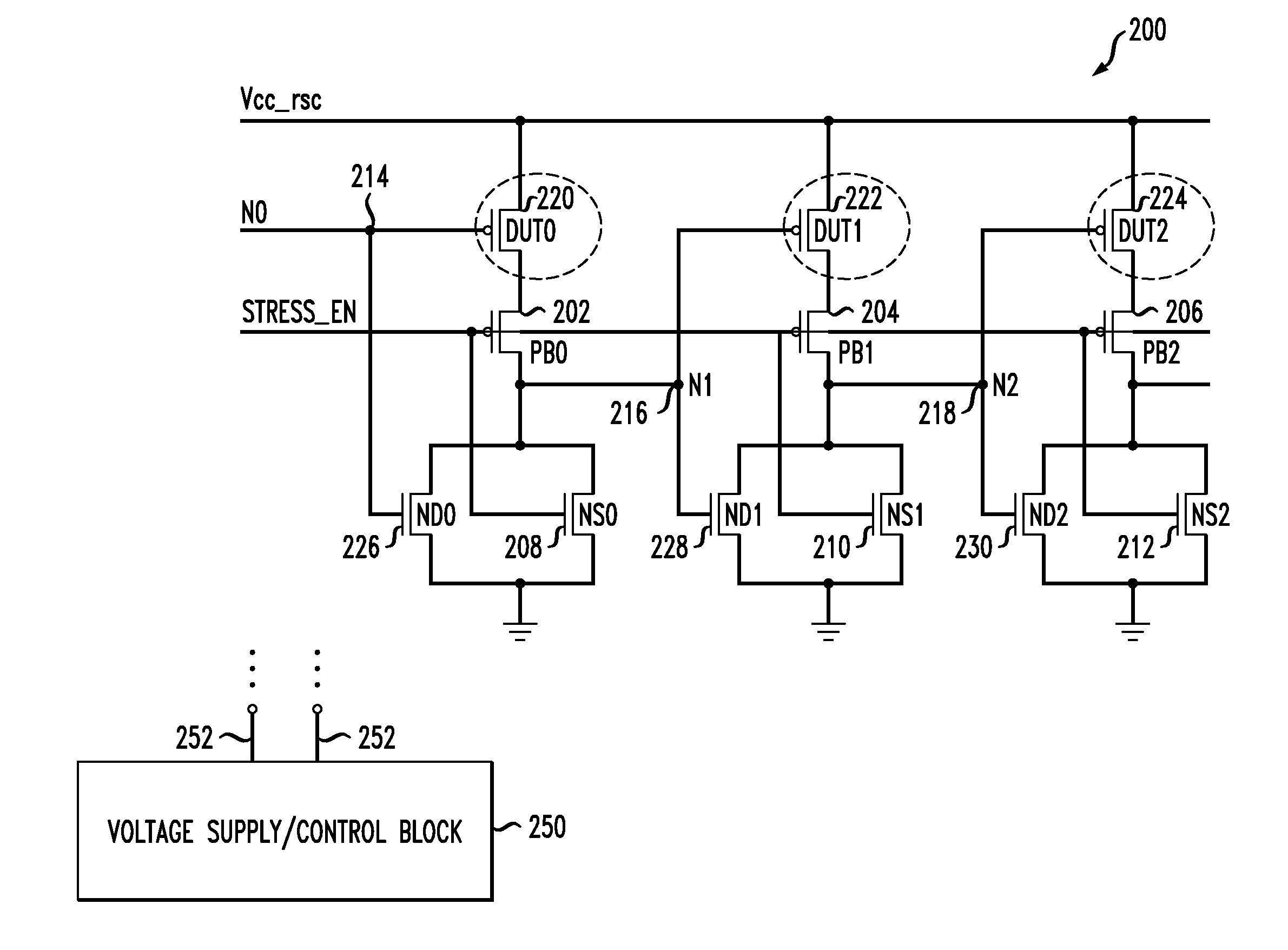
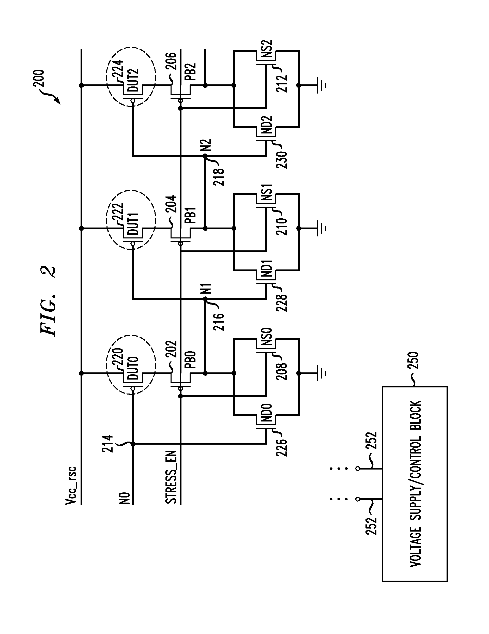
[0032]One or more embodiments of the invention provide test structures and schemes that enable efficient characterization and analysis of both PBTI and NBTI effects, and their impact on circuits. Since the dependencies, mechanisms and magnitudes of PBTI and NBTI may differ, it is advantageous to be able to isolate the impact of each of these two effects.
[0033]In one or more embodiments, the simplicity of the ring-oscillator based configuration is maintained, while the two types of devices (n and p) are isolated using simple switches and pre-bias circuits. In measurement mode, these switches are closed and pre-bias circuits are disabled, so that the circuit operates as a ring-oscillator. In stress mode, these switches are open; thereby eliminating the interaction between the two types of stressed devices, while the requisite stress voltages are applied via the pre-bias circuits. One or more embodiments of the invention isolate the contributions of the two effects; this isolation is b...
PUM
 Abstract
Description
Claims
Application Information