Multilayer printed wiring board

a printed wiring board and multi-layer technology, applied in the association of printed circuit non-printed electric components, semiconductor/solid-state device details, electrical apparatus construction details, etc., can solve the problems of easy electric potential instantaneous drop, difficult inability to achieve satisfactory decoupling effect, etc., to achieve easy design, easy to prevent instantaneous electric potential drop, and increase the capacitance of the layered capacitor portion

Active Publication Date: 2010-01-19
IBIDEN CO LTD
View PDF16 Cites 22 Cited by
  • Summary
  • Abstract
  • Description
  • Claims
  • Application Information

AI Technical Summary

Benefits of technology

[0004]The present invention has been conceived in view of the above problems, and it is an object of the present invention to provide a multilayer printed wiring board in which a satisfactory decoupling effect can be achieved, and malfunctioning of a semiconductor device can also be satisfactorily prevented.
[0016]The multilayer printed wiring board of the present invention may further include a stress relief portion which is provided between the mounting portion and the layered capacitor portion and which is made of an elastic material. In this structure, even when a stress due to a difference in thermal expansion is generated between the semiconductor device mounted on the mounting portion and the layered capacitor portion or the built-up portion, the stress relief portion absorbs the stress, and thus problems such as a decrease in the connection reliability and a decrease in the insulation reliability do not easily occur. Although cracks are easily generated in the high-dielectric layer of the layered capacitor portion because of its small thickness and brittleness, the presence of the stress relief portion can prevent the generation of cracks. In this case, the stress relief portion may be provided in an area only directly under the semiconductor device mounted on the mounting portion. A problem of a stress due to a difference in thermal expansion mainly occurs in the area directly under the semiconductor device. Therefore, when the stress relief portion is provided on this area, the cost of the material can be reduced. Examples of the material of the stress relief portion include, but are not particularly limited to, organic resin sheets such as a modified epoxy resin sheet, a polyphenylene ether resin sheet, a polyimide resin sheet, a cyanoester resin sheet, and an imide resin sheet. These organic resin sheets may contain a thermoplastic resin such as a polyolefin resin or a polyimide resin; a thermosetting resin such as a silicone resin; or a rubber resin such as styrene-butadiene rubber (SBR), acrylonitrile-butadiene rubber (NBR), or a urethane. These organic resin sheets may also contain fibers, fillers, or flakes made of an inorganic material such as silica, alumina, or zirconia. The stress relief portion preferably has a Young's modulus in the range of 10 to 1,000 MPa. In the case where the Young's modulus of the stress relief portion is within the above range, even when a stress due to a difference in the coefficient of thermal expansion between the semiconductor device mounted on the mounting portion and the layered capacitor portion is generated, the stress can be relieved.

Problems solved by technology

However, since the layered capacitor portion disclosed in Patent Document 1 includes a dielectric layer made of an organic resin containing an inorganic filler such as barium titanate, the dielectric layer cannot have a satisfactorily high capacitance.
Accordingly, it is difficult to achieve a satisfactory decoupling effect under a condition that the frequency for switching between the on and off states of a semiconductor device is high, i.e., in the range of several gigahertz to several tens of gigahertz in which an instantaneous drop in the electric potential easily occurs.
In addition, malfunctioning of the semiconductor device after a heat cycle test cannot be satisfactorily prevented.

Method used


Image

  • Multilayer printed wiring board
  • Multilayer printed wiring board
  • Multilayer printed wiring board

Examples


first embodiment

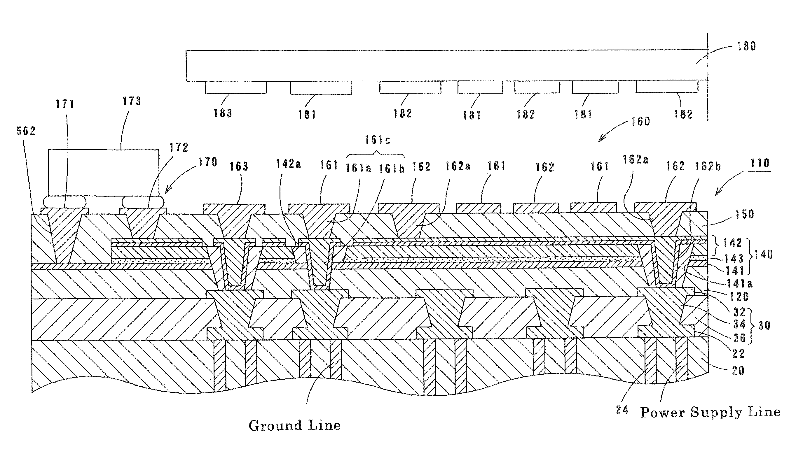
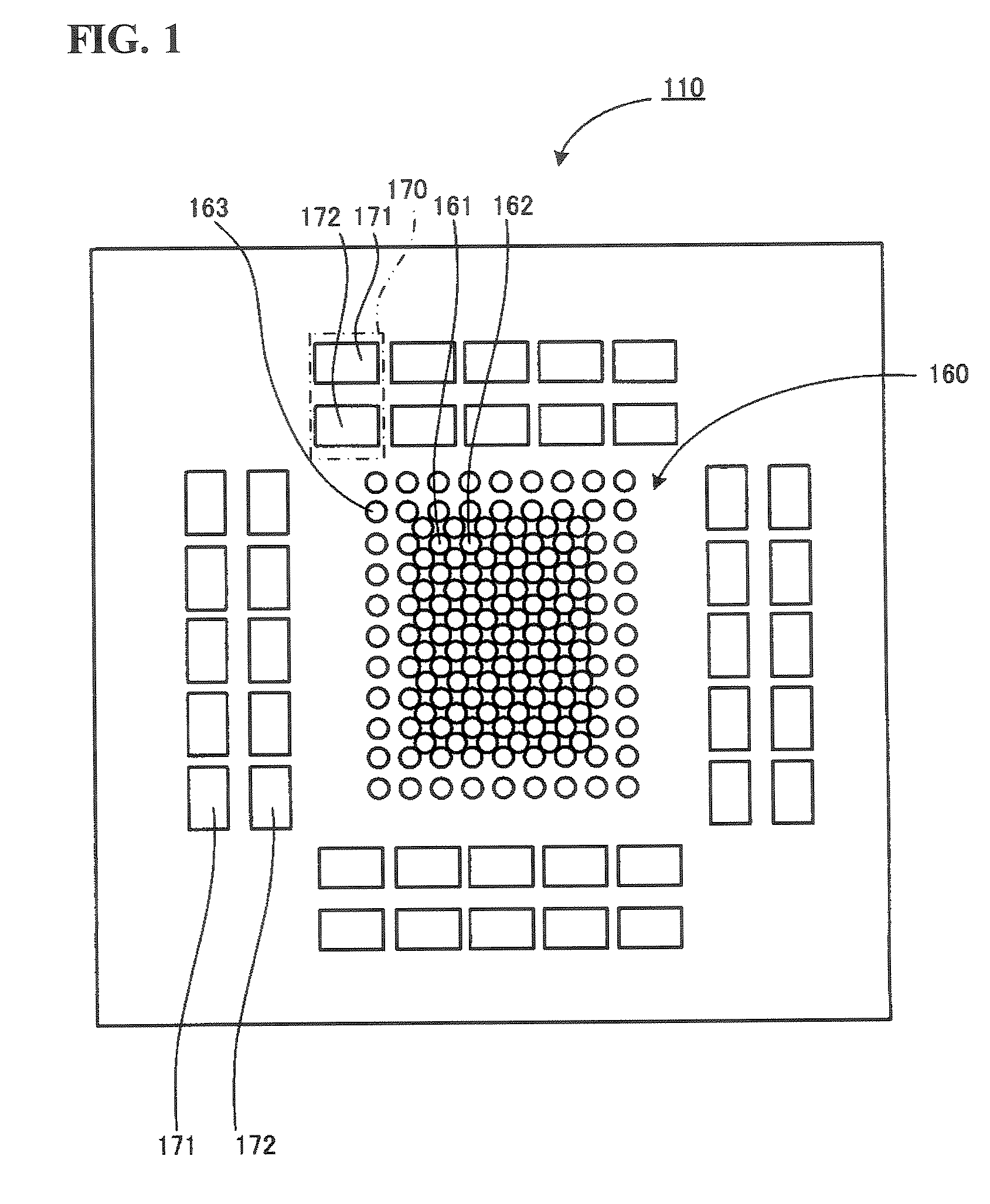
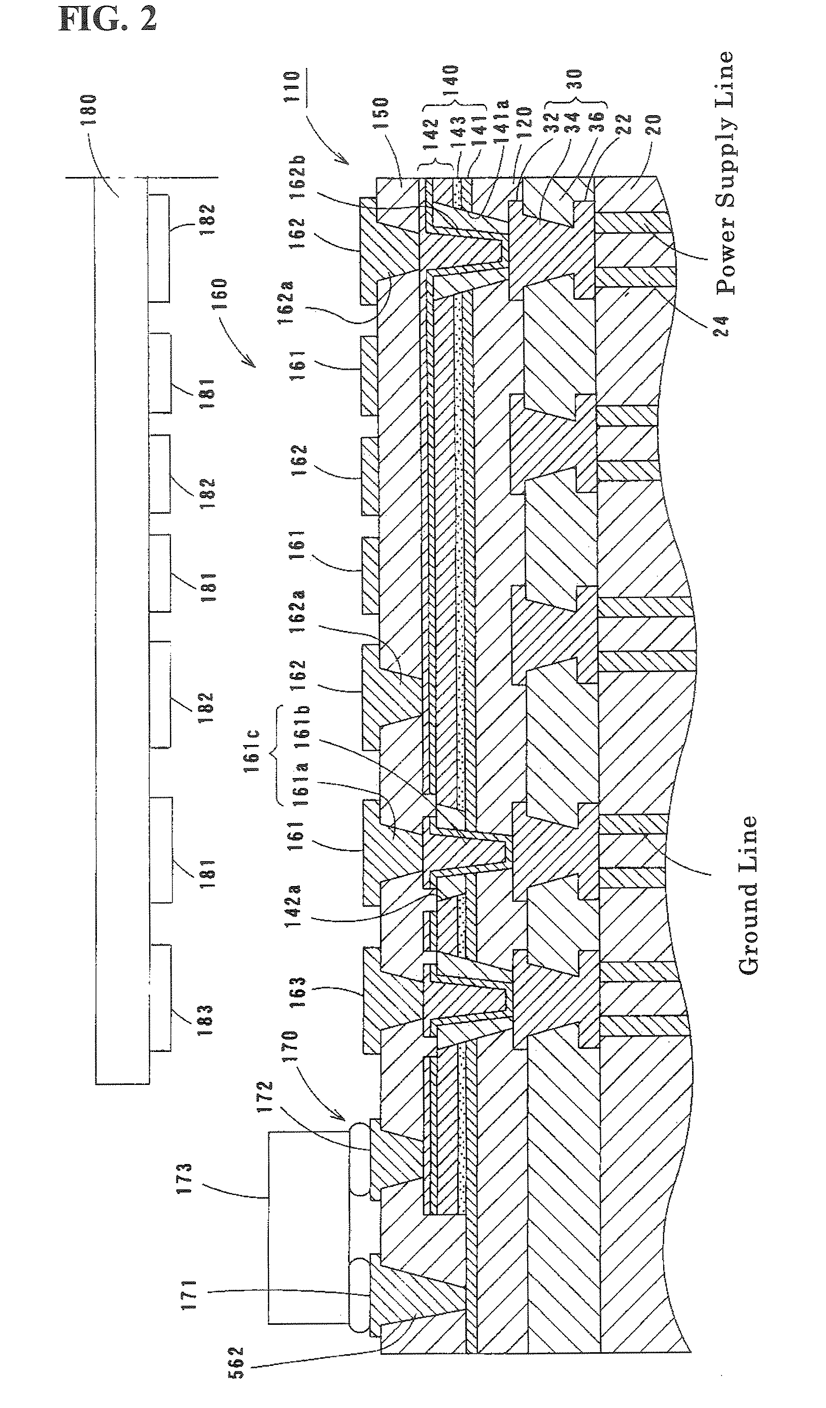
[0030]Embodiments of the present invention will now be described with reference to the drawings. FIG. 1 is a plan view of a multilayer printed wiring board 110 according to a first embodiment of the present invention, FIG. 2 is a longitudinal cross-sectional view of the multilayer printed wiring board 110 (which shows only the part to the left of the center line), and FIG. 3 is a schematic perspective view showing a layered capacitor portion 140.

[0031]As shown in FIG. 2, the multilayer printed wiring board 110 of this embodiment includes a core substrate 20 in which wiring patterns 22 provided on the upper surface and the lower surface of the substrate are electrically connected to each other via through-hole conductors 24; a built-up portion 30 in which a plurality of wiring patterns 32 and 22, which are stacked with a resin insulating layer 36 therebetween, are electrically connected through via holes 34, the built-up portion 30 being provided on the upper surface of the core subs...

second embodiment

[0060]FIG. 8 is a longitudinal cross-sectional view of a multilayer printed wiring board 210 (which shows only the part to the left of the center line) according to a second embodiment. As shown in FIG. 8, the multilayer printed wiring board 210 of this embodiment includes a core substrate 20 similar to that of the first embodiment; a built-up portion 30 in which a wiring pattern 22 and a wiring pattern 32, which are stacked with a resin insulating layer 36 therebetween, are electrically connected through via holes 34, the built-up portion 30 being provided on the upper surface of the core substrate 20; an interlayer insulating layer 220 stacked on the built-up portion 30; a layered capacitor portion 240 which is stacked on the interlayer insulating layer 220 and which includes a first layered electrode 241, a second layered electrode 242, and a high-dielectric layer 243 provided between the first layered electrode 241 and the second layered electrode 242; an interlayer insulating l...

experimental examples 1 to 5

[0075]In Experimental Examples 1 to 5, in the first embodiment, the number of times the steps of spin-coating, drying, and sintering of the procedure (4) in the process of preparing the high-dielectric sheet were repeated was four, and a high-dielectric layer 143 having a thickness of 0.12 μm was prepared. By varying the number of second rod-shaped conductors 162b and the number of first rod-shaped conductors 161c of the multilayer printed wiring board 110 shown in FIG. 2 in each experimental example, the ratio of the number of second rod-shaped conductors 162b to the number of power supply pads 162 and the ratio of the number of first rod-shaped conductors 161c to the number of ground pads 161 were controlled as shown in Table 1. Each of the number of power supply pads 162 and the number of ground pads 161 was 10,000. By adjusting the sizes of passing holes 141a and 142a, the capacitance at a position directly under a die of the layered capacitor portion 140 was controlled to 3.8 μ...


PUM

PropertyMeasurementUnit
distanceaaaaaaaaaa
Young's modulusaaaaaaaaaa
capacitanceaaaaaaaaaa

Abstract

A multilayer printed wiring board includes a mounting portion supporting a semiconductor device and a layered capacitor portion including first and second layered electrodes and a ceramic high-dielectric layer therebetween. The first layered electrode is connected to a ground line and the second layered electrode is connected to a power supply line. The ratio of number of via holes, each constituting a conducting path part electrically connecting a ground pad to the ground line of a wiring pattern and passing through the second layered electrode in non-contact, to number of ground pads is 0.05 to 0.7. The ratio of number of second rod-shaped conductors, each constituting a conducting path part electrically connecting a power supply pad to the power supply line of the wiring pattern and passing through the first layered electrode in non-contact, to number of power supply pad is 0.05 to 0.7.

Description

TECHNICAL FIELD[0001]The present invention relates to a multilayer printed wiring board including a built-up portion in which a plurality of wiring patterns that are stacked with insulating layers therebetween are electrically connected through via holes provided in the insulating layers.BACKGROUND ART[0002]Hitherto, various types of structures of a multilayer printed wiring board including a built-up portion in which a plurality of wiring patterns that are stacked with insulating layers therebetween are electrically connected through via holes provided in the insulating layers have been proposed. For example, in such a multilayer printed wiring board, when a semiconductor device mounted is switched between the on and off states at a high speed, switching noise may be generated, resulting in an instantaneous drop in the electric potential of a power supply line. In order to suppress such an instantaneous drop in the electric potential, connection of a capacitor portion between the p...

Claims


Application Information

Patent Timeline
Patent Type & Authority Patents(United States)
IPC IPC(8): H05K7/00
CPCH05K1/162H01L24/16Y10T29/49133H01L2924/0102H01L2924/01025H01L2924/01057H01L2924/01078H01L2924/01079H01L2924/14H01L2924/19041H01L2924/19043H01L2924/19105H01L2924/30105H01L2924/30107H01L2924/3011H05K1/113H05K3/4602H05K3/4652H05K2201/0175H05K2201/09509H05K2201/09518H05K2201/096H05K2201/09718H05K2201/10674H01L2924/01012H01L2924/01019Y10T29/49162H01L2224/16H01L2924/12042H01L2924/00014H01L2924/00011H01L2924/00H01L2224/0401H05K3/46H01L23/12H01L21/3205H05K7/00H05K1/18
Inventor KARIYA, TAKASHITANAKA, HIRONORI
Owner IBIDEN CO LTD
Why Eureka
Try Eureka