Piezoelectric actuator for tunable electronic components

a technology of electronic components and actuators, applied in piezoelectric/electrostrictive/magnetostrictive devices, piezoelectric/electrostriction/magnetostriction machines, electrical apparatus, etc., can solve the problems of inability to maintain a high-q or quality factor, inherently lossy methods, and bulky structures, so as to facilitate the fabrication of custom laterals and reduce costs. , the effect of reducing the cos

Inactive Publication Date: 2010-02-02
HRL LAB
View PDF56 Cites 13 Cited by
  • Summary
  • Abstract
  • Description
  • Claims
  • Application Information

AI Technical Summary

Benefits of technology

[0020]A first advantage of the present invention is that the layered piezoelectric actuator can be integrated with a membrane structure. The integration process between the actuator and the membrane structure is compatible both with commercially available piezoelectric actuators and with thin film actuators that can be deposited at the time of fabrication.
[0021]A second advantage of the present invention is that the design of the actuator offers the flexibility of optimizing the membrane displacement and response time, which can be matched to the needs of the particular application.
[0022]A third advantage of the present invention is that applications that require cooling of the components to low temperatures (such as 77° K) do not pose a problem, as any thermal mismatch is minimized, given that the actuator can be in the form of a thin film (e.g. 10 microns thick).
[0023]Additionally, the actuator wafer level fabrication process makes it possible to easily fabricate many hundreds or thousands of elements simultaneously. More particularly, the present invention is compatible with miniaturization and cleanroom processing techniques. This enables the fabrication of hundreds or thousands of membrane-actuator components on a single wafer, significantly lowering their cost. The final lateral dimensions can be sub-mm. The compatibility of the present invention with cleanroom processing techniques greatly facilitates the fabrication of custom lateral and vertical dimensions for the membrane and piezoelectric actuator. The actuator thickness can, therefore, be optimized to achieve a substantial vertical travel range (about ±50 microns), while keeping the lateral dimensions relatively small (about 5-10 mm). This significantly enhances the tuning ability of the device. The prior art does not indicate the capability of any extensive travel range.
[0024]A further advantage of the present invention is that it significantly extends the tuning range for microwave components by allowing precise control of the membrane position at arbitrarily small separations from the substrate.
[0025]Additionally, the present invention is compatible with miniaturization of the various components, thereby significantly reducing the response time for the tuning process, as well as extending the applicability to higher frequency applications. More particularly, the piezoelectric layers can be optimally designed and supported on the membrane borders to prevent any mass loading. This gives a higher resonance frequency for the membrane-actuator assembly, thereby providing a short response time for the tuning process.

Problems solved by technology

These methods are inherently lossy and cannot maintain a high-Q, or quality factor, over the entire range of tunable frequencies.
This makes the structure bulky and difficult to integrate with the membrane and circuit.
However, the technique has a severe limitation on the travel range of the membrane due to a nonlinear increase in the deflection force as the gap becomes small.
As a result, the membrane collapses onto the substrate when the separation is about ⅓ of the original gap, preventing accurate control of the membrane position.
This severely limits the tuning range of the component, which is strongly dependent on the membrane position as the separation becomes small.
However, this requires a significantly higher actuation voltage and still does not offer a precise control of the membrane position.
Additionally, other aspects of the circuit design may place stringent constrains on the position of the electrodes, which would make this technique unfeasible.
Additionally, the process disclosed in Imada is not compatible with wafer level photolithographic techniques.
A further disadvantage is that the cantilevers in Imada cannot be designed for use as actuators to produce static membrane deflections, as the force generated is quite small.
This renders the actuator useless for tuning applications, for which much larger (about 20 microns) deflections are desirable.
An enlargement of the structure to about 10 mm lateral dimensions does not work, as the membrane material is fragile at those sizes.
A first disadvantage is that the movement caused by the piezoelectric layer is unidirectional only.
A second disadvantage is that the changing air gap between the substrate and the ground plane is not uniform.
A third disadvantage is that the device is not compatible with miniaturization and cleanroom processing techniques, so that custom lateral and vertical dimensions for the actuator cannot be fabricated.

Method used


Image

  • Piezoelectric actuator for tunable electronic components
  • Piezoelectric actuator for tunable electronic components
  • Piezoelectric actuator for tunable electronic components

Examples


first embodiment

[0050]According to the process, the actuator is purchased commercially and then combined with the membrane. Combination of the commercially available actuator (for example a PI Ceramic PL-122.251 actuator, about 0.5 mm thick) with the membrane can be obtained by means of a thin layer of adhesive, about 1 micron thick. The use of the thin layer of adhesive will be described in better detail with reference to FIG. 6(c)(1).

second embodiment

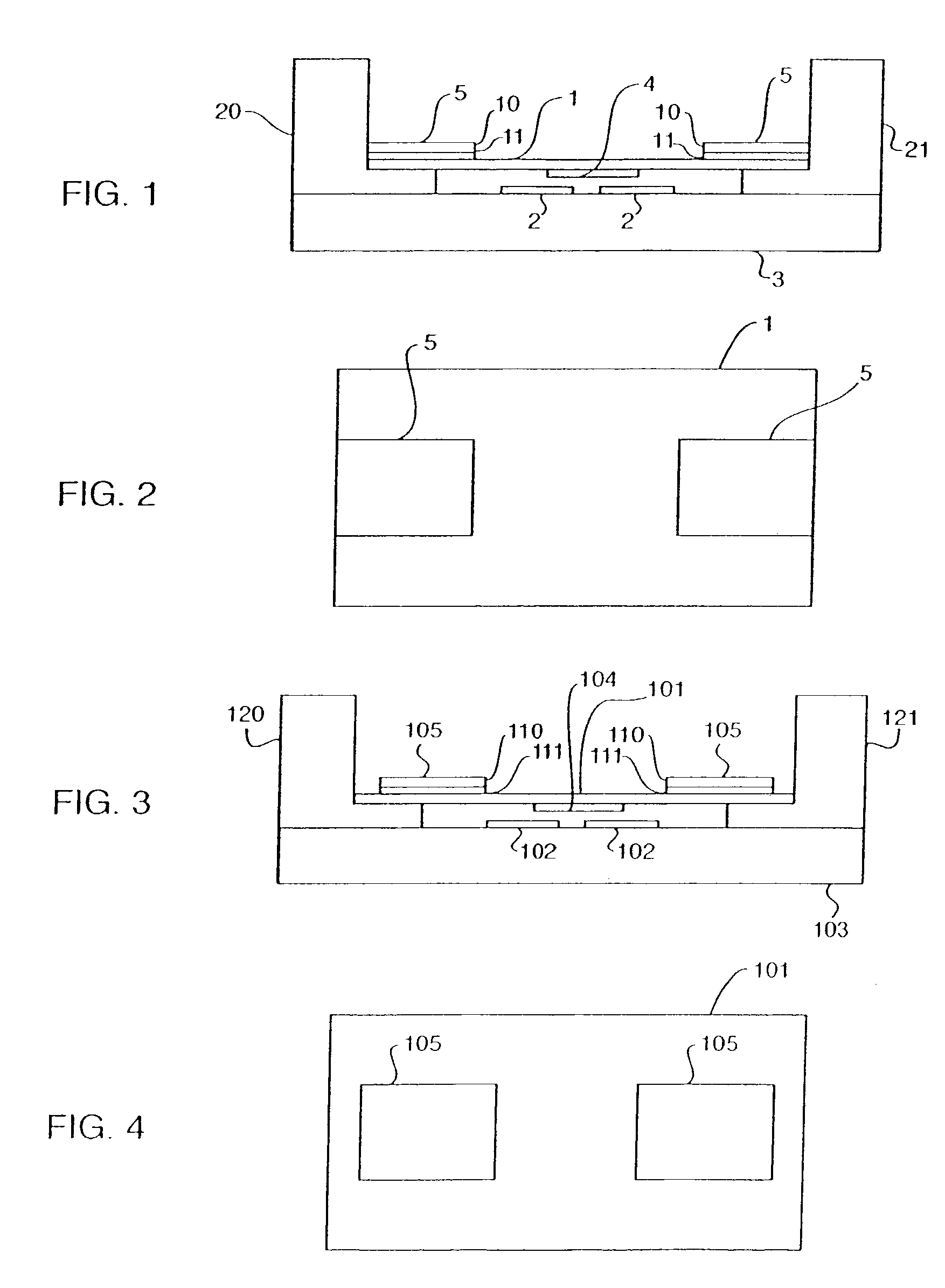
[0051]According to the process, the actuator is made in-house and integrated with the membrane during the fabrication process. Note that the actuating assembly shown in FIGS. 1-4 may be fabricated by processes other than those depicted in the following figures. Further, while the following figures depict multiple separate fabrication steps, alternative fabrication processes may allow several separate steps to be combined into fewer steps. Finally, alternative fabrication processes may use a difference sequence of steps.

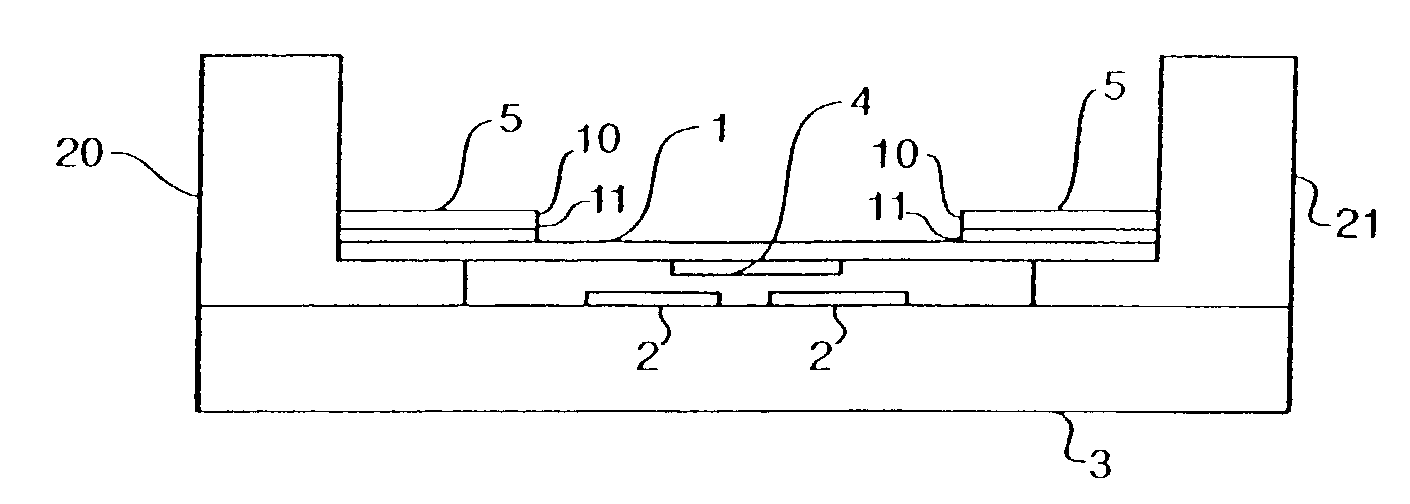
[0052]FIGS. 6(a)-6(e) show a process according to the first embodiment of the present invention, where a commercial piezoelectric actuator is assembled with a membrane. In each step of the process, generally known microfabrication techniques, such as masking, etching, deposition, and lift-off are used.

[0053]FIG. 6(a) shows a first step, where a trench 41 having a trench depth is patterned into the silicon wafer substrate 3. The trench depth is equal to the height of t...


PUM

PropertyMeasurementUnit
sizesaaaaaaaaaa
thicknessesaaaaaaaaaa

Abstract

An actuating assembly for tuning a circuit and a process for forming a carrier substrate containing a membrane, a conductive layer, and piezoelectric actuators are disclosed. The actuating assembly comprises a membrane overlying a circuit to be tuned, a conductive element connected with the membrane, and a piezoelectric arrangement. Changes in shape of the piezoelectric arrangement allow a deflection of the membrane and a corresponding controllable upward or downward movement of the conductive element. In the process, a membrane and a piezoelectric structure are formed on a substrate.

Description

CLAIM OF BENEFIT OF PROVISIONAL APPLICATION[0001]This application claims the benefit of U.S. provisional application Ser. No. 60 / 420,174 filed on Oct. 21, 2002, which is incorporated herein by reference in its entirety.STATEMENT REGARDING FEDERALLY SPONSORED RESEARCH OR DEVELOPMENT[0002]The present invention was made with support from the United States Government under Contract No. MDA972-00-C-0030, awarded by the DARPA TASS Program. The U.S. Government has certain rights in the invention.CROSS-REFERENCE TO RELATED APPLICATIONS[0003]The present document is related to the copending and commonly assigned patent application documents entitled “Variable Capacitance Membrane Actuator for Wide Band Tuning Microstrip Resonators and Filters,” Ser. No. 10 / 421,302, and “Piezoelectric Switch for Tunable Electronic Components,” Ser. No. 10 / 421,327, which are all filed of even date herewith. The contents of these related applications arc hereby incorporated by reference herein.FIELD OF THE INVEN...

Claims


Application Information

Patent Timeline
Patent Type & Authority Patents(United States)
IPC IPC(8): H01L41/08H01G5/18H01L41/09H01L41/22
CPCH01G5/18H01L41/313H01L41/25H01L41/0933Y10T29/42H10N30/2041H10N30/03H10N30/073
Inventor MEHTA, SARABJIT
Owner HRL LAB
Why Eureka
Try Eureka