Semiconductor device and manufacturing method thereof

a semiconductor and manufacturing method technology, applied in the direction of transistors, solid-state devices, instruments, etc., can solve the problems of reducing the wiring width, difficult finer processing of the first-layer wiring lines b>139/b>a and b>139/b>b, and increasing so as to reduce the wiring density of the first-layer wiring lines, improve the flexibility of the circuit layout, and reduce the number of manufacturing processes.

Inactive Publication Date: 2010-02-02
LONGITUDE SEMICON S A R L
View PDF8 Cites 6 Cited by
  • Summary
  • Abstract
  • Description
  • Claims
  • Application Information

AI Technical Summary

Benefits of technology

[0016]In light of the above circumstances, an object of the present invention is to provide (i) a semiconductor device, which can be manufactured without increasing the number of manufacturing processes, and contributes to the reduction of the wiring density of first-layer wiring lines, improved flexibility in the circuit layout, and the reduction of parasitic resistance or parasitic capacitance of the first-layer wiring lines, and (ii) a manufacturing method thereof.
[0060]In accordance with the semiconductor device and the manufacturing method thereof, the assist wiring line is provided in the peripheral circuit area and at the same layer position as that of the landing pad provided at the bottom surface of the capacitor. Therefore, it is possible to reduce the wiring density with respect to the first-layer wiring line, provide a required flexibility in the circuit layout, and reduce parasitic resistance or parasitic capacitance of the first-layer wiring line. In addition, the semiconductor device can be manufactured without increasing the number of manufacturing processes.

Problems solved by technology

Therefore, if the integration of the semiconductor device further proceeds and the layout size (i.e., F value) is decreased, fine processing of the first-layer wiring lines 139A and 139B becomes more difficult.
Therefore, in such an area, finer processing of the first-layer wiring lines 139A and 139B is difficult.
Additionally, accompanied with a further decrease in the wiring width, an RC delay appears.

Method used


Image

  • Semiconductor device and manufacturing method thereof
  • Semiconductor device and manufacturing method thereof
  • Semiconductor device and manufacturing method thereof

Examples


first embodiment

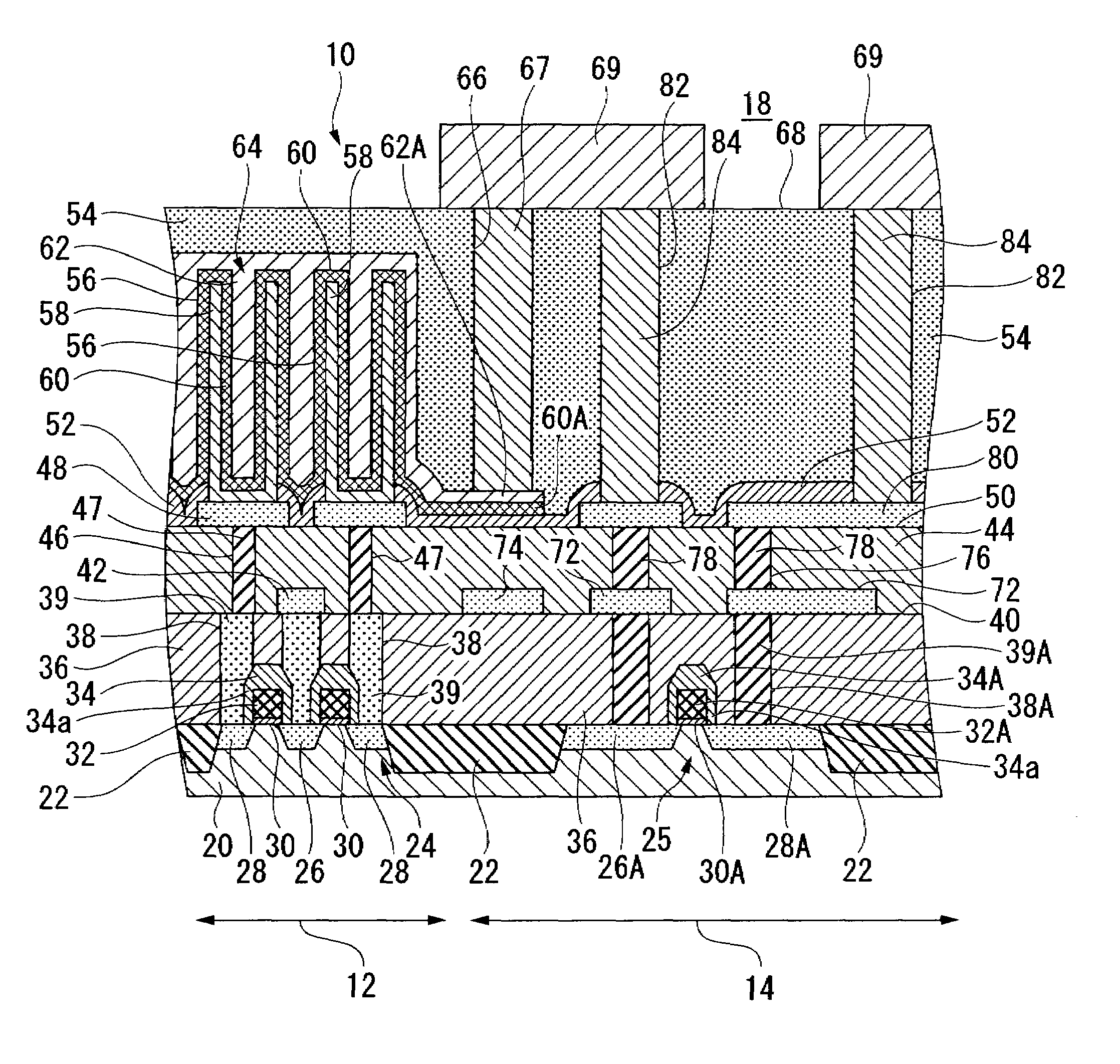
[0078]Below, a semiconductor device having a peripheral circuit area of a DRAM cell and the manufacturing method thereof will be explained as a first embodiment of the present invention.

[0079]FIG. 1 is a longitudinal sectional view showing a semiconductor device 10 which includes a memory (cell) area and a peripheral circuit area (or a logic circuit area) of a DRAM cell. That is, in the semiconductor device 10, a memory cell area 12 and a peripheral circuit area 14 of a DRAM cell are provided on a single semiconductor substrate 20.

[0080]The memory structure of the DRAM cell will be explained below.

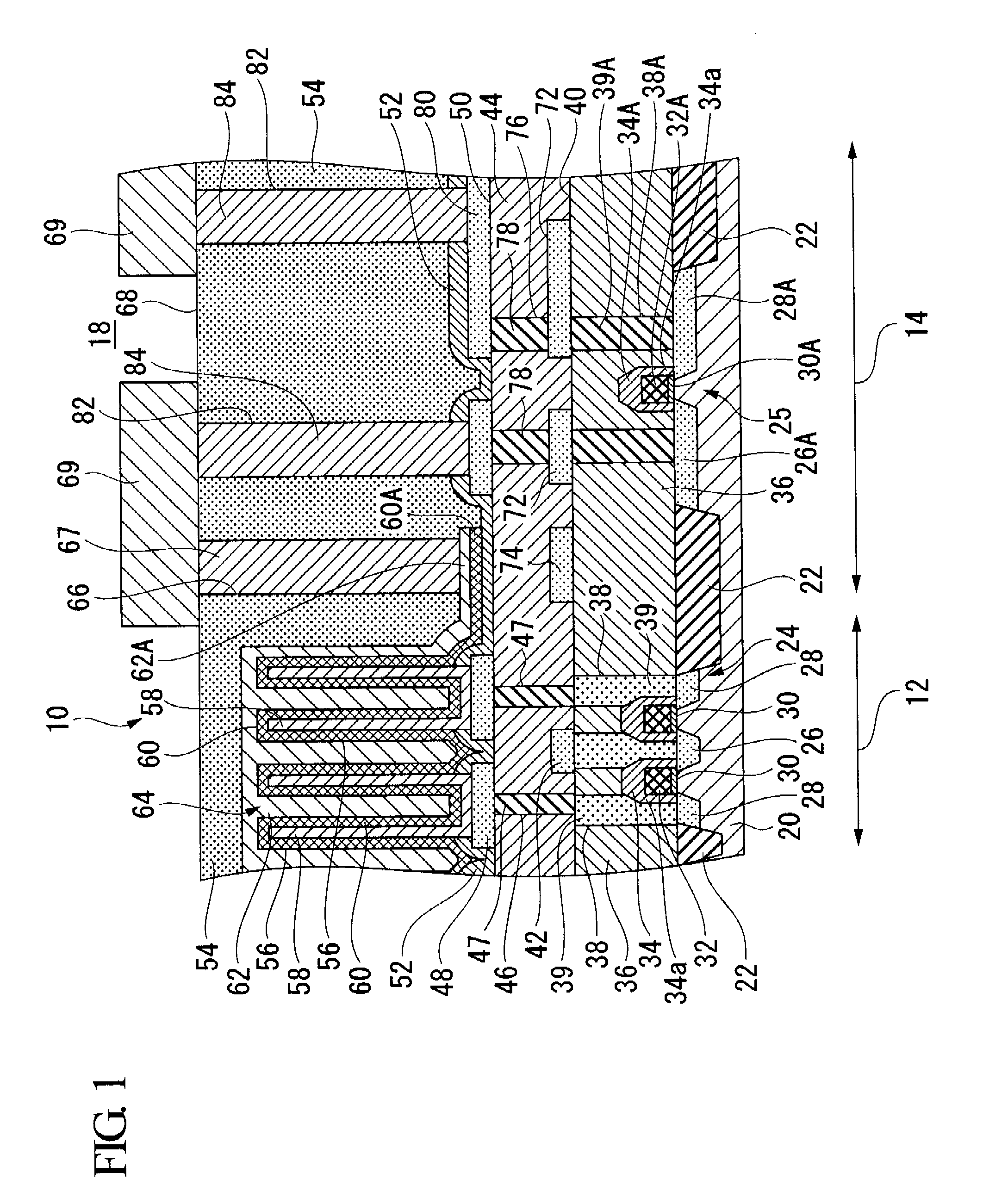
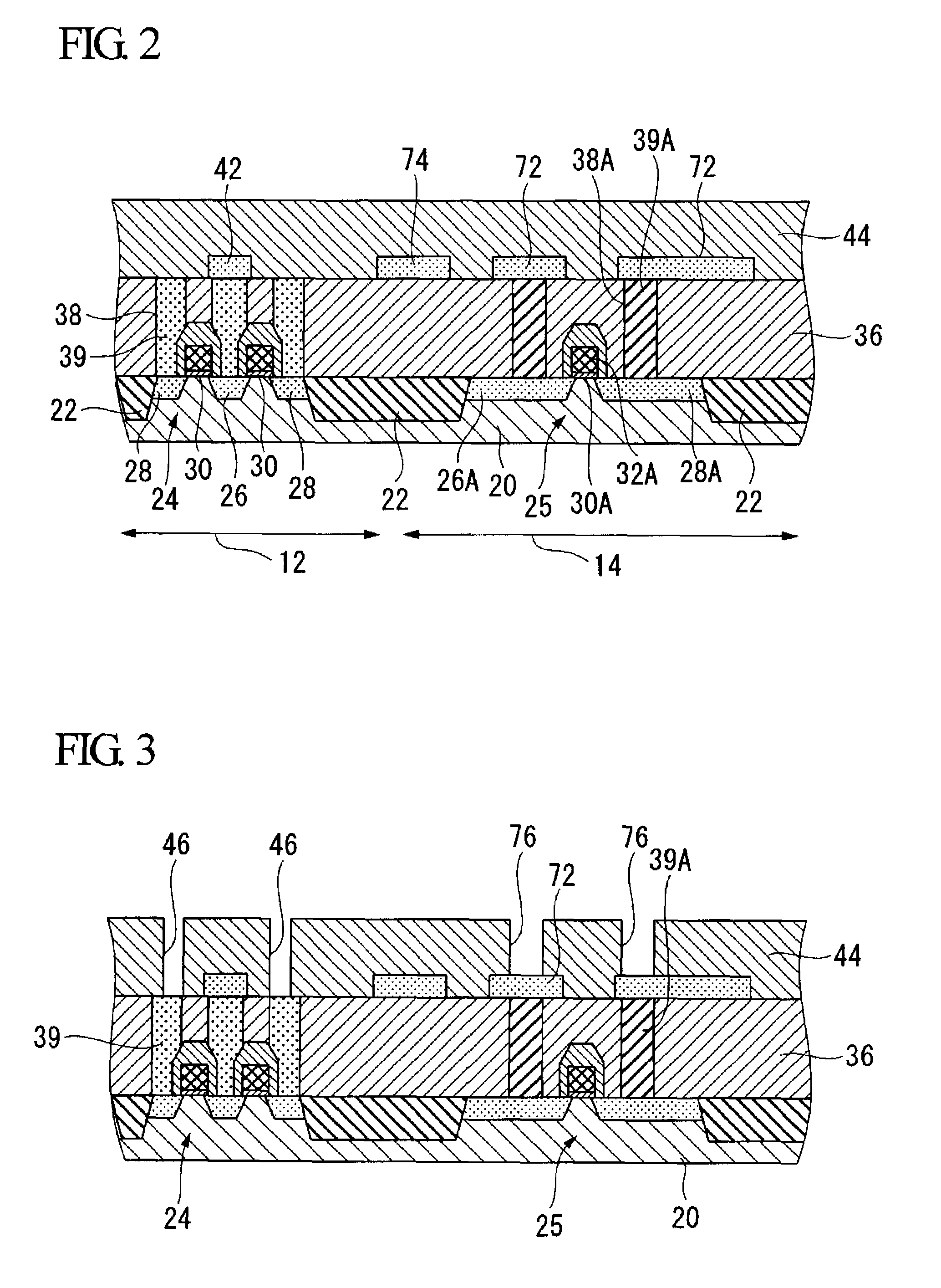
[0081]The semiconductor substrate 20 is made of silicon in which p-type impurities are doped. By means of separating insulating areas 22, a transistor forming area of the semiconductor substrate 20 is separated from the other areas in an insulating manner. In an active region interposed between the separating insulating areas 22, diffusion layer areas in which n-type impurities are doped a...

second embodiment

[0130]FIG. 15 is a general sectional view showing a semiconductor device 501 as a second embodiment of the present invention. In comparison with the first embodiment, the semiconductor device 501 of the present embodiment has a distinctive extension structure of the upper electrode 62 on a side of the capacitor 64. The other parts are identical to those in the first embodiment, and explanations thereof are omitted.

[0131]As shown in FIG. 15, in the semiconductor device 501 of the second embodiment, an assist wiring line 80A is formed by means of patterning on the main surface 50 of the second inter-layer insulating film 44, in a manner such that it extends to the boundary between the memory cell area 12 and the peripheral circuit area 14. The upper electrode 62 with respect to the deep-hole cylinders 56 for forming the capacitor 64 extends on the silicon nitride film 52 which covers the assist wiring line 80A. The assist wiring line 80A is connected (i) via a second metal contact plu...


PUM


Abstract

In a memory cell area of a semiconductor device, first, second, and third inter-layer insulating films respectively cover a cell transistor, a bit wiring line, and a capacitor which are connected to each other. In an adjacent peripheral circuit area, a peripheral-circuit transistor is covered with the first inter-layer insulating film, a first-layer wiring line connected to the peripheral-circuit transistor is provided on the first inter-layer insulating film and covered with the second inter-layer insulating film, and a second-layer wiring line is provided on the third inter-layer insulating film. In the memory cell area, a landing pad is provided on the second inter-layer insulating film and between the capacitor and a contact plug for connecting the capacitor to the cell transistor. An assist wiring line connected to the first-layer wiring line is provided on the main surface of the second inter-layer insulating film, on which the landing pad is provided.

Description

BACKGROUND OF THE INVENTION[0001]1. Field of the Invention[0002]The present invention relates to a semiconductor device including memory cells and a peripheral circuit and / or a logic circuit of a DRAM (dynamic random access memory), and a manufacturing method of the semiconductor device.[0003]Priority is claimed on Japanese Patent Application No. 2007-090099, filed Mar. 30, 2007, the contents of which are incorporated herein by reference.[0004]2. Description of the Related Art[0005]Conventional semiconductor devices include general DRAMs, embedded DRAMs, and the like. In a peripheral circuit area of a general DRAM or a logic circuit area of an embedded DRAM, in order to make transistors conductive to each other, (i) first-layer wiring lines formed on the same layer as that on which a bit wiring line of a memory cell is provided below a capacitor, and (ii) second-layer wiring lines and third-layer wiring lines, which are provided above the capacitor, are electrically connected so as ...

Claims


Application Information

Patent Timeline
Patent Type & Authority Patents(United States)
IPC IPC(8): G11C5/06
CPCH01L27/10894H01L28/91H10B12/09
Inventor NAKAMURA, YOSHITAKAIZAWA, MITSUTAKA
Owner LONGITUDE SEMICON S A R L
Why Eureka
Try Eureka