Storage device and semiconductor device

a storage device and semiconductor technology, applied in the field of semiconductor devices, can solve the problems of delay in practical application, uv rays need to be used to erase data, and drawbacks of eproms

Inactive Publication Date: 2010-02-09
SEMICON ENERGY LAB CO LTD
View PDF7 Cites 9 Cited by
  • Summary
  • Abstract
  • Description
  • Claims
  • Application Information

AI Technical Summary

Benefits of technology

[0008]In view of the above problem, it is an object of the present invention to provide a storage device and a semiconductor device at low cost which are nonvolatile, easily manufactured, and capable of storing and erasing information.
[0021]According to the present invention, data can be written, erased, and rewritten arbitrarily. Moreover, inexpensive storage device and semiconductor device having minute structures can be provided by applying the present invention.

Problems solved by technology

With the progress of information technology in recent years, memories capable of storing, erasing, and reading a larger amount of data at high speed have been demanded, and size reduction, cost reduction, and integration of nonvolatile memories have been important issues.
However, an EPROM has a drawback that UV rays need to be used to erase data.
However, there has been a delay in practical application of this FeRAM, resulting from technical difficulty in thinning a ferroelectric film.

Method used


Image

  • Storage device and semiconductor device
  • Storage device and semiconductor device
  • Storage device and semiconductor device

Examples


embodiment mode 1

[0050]This embodiment mode will describe a structural example of a storage device (hereinafter also referred to as a storage circuit or an organic memory) in which an organic compound is provided between two conductive layers, with reference to drawings.

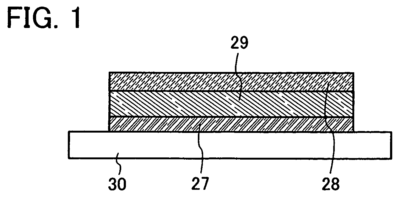
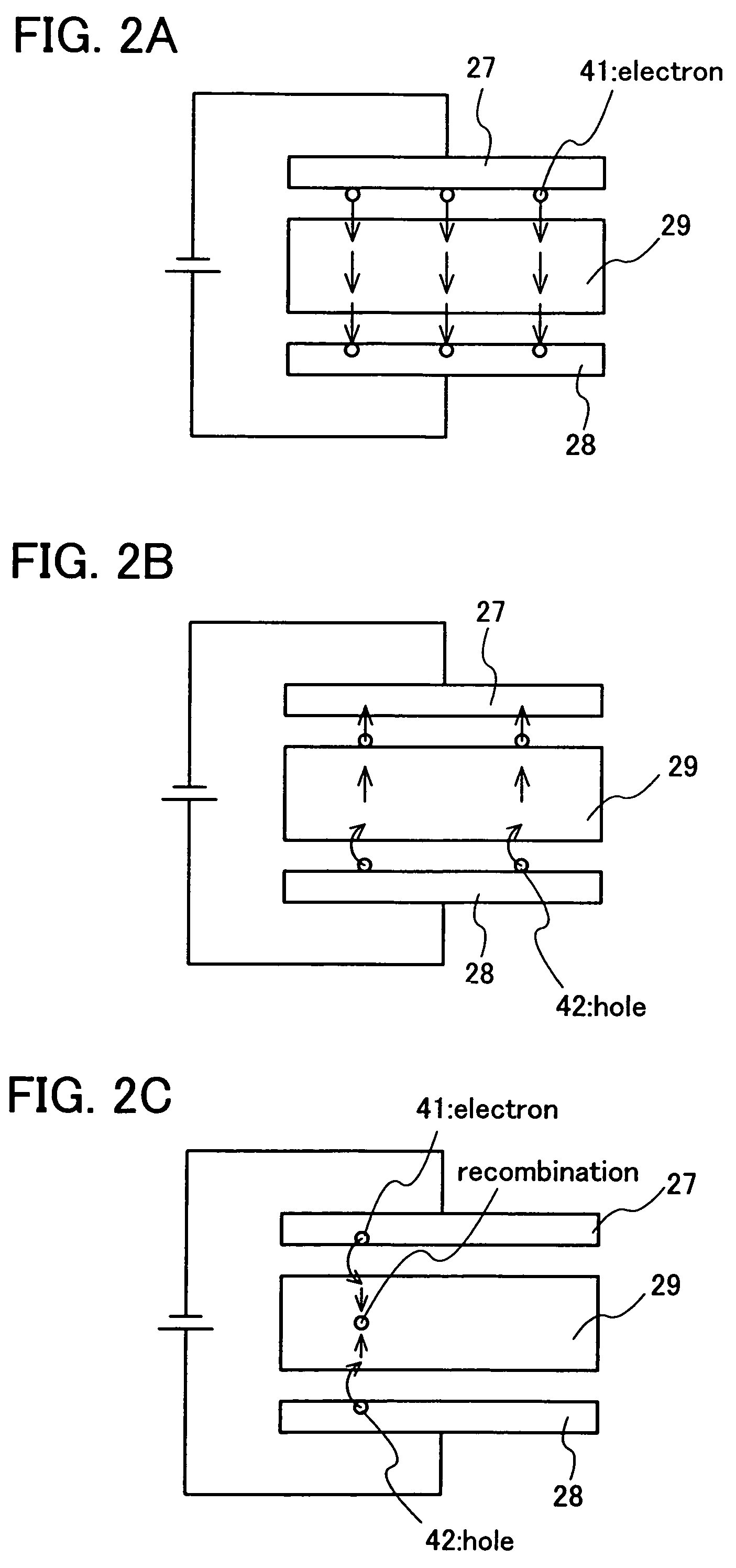
[0051]As shown in FIG. 1, a glass substrate made of barium borosilicate glass, aluminoborosilicate glass, or the like; a quartz substrate; a ceramic substrate; or the like can be used as a substrate 30. A metal substrate containing stainless steel or a semiconductor substrate over which an insulating layer is formed may also be used. Although a substrate made of flexible synthetic resin such as plastic, for example PET, tends to have lower allowable temperature limit than the above substrates in general, the substrate made of flexible synthetic resin can also be used as long as the substrate can resist process temperature in manufacturing steps. It is to be noted that a surface of the substrate 30 may be flattened by polishing by a C...

embodiment mode 2

[0073]This embodiment mode will describe a structural example of a storage circuit including an organic compound layer in a storage element portion with reference to drawings. More specifically, this embodiment mode will show a case of a storage circuit having a passive matrix structure.

[0074]FIG. 5A shows a structural example of a semiconductor device of the present invention, which includes a memory cell array 22 in which memory cells 21 are arranged in a matrix form; a bit line driver circuit 26 having a column decoder 26a, a reading circuit 26b, and a selector 26c; a word line driver circuit 24 having a row decoder 24a and a level shifter 24b; and an interface 23 having a writing circuit and the like to communicate with the outside. It is to be noted that the structure of the storage circuit 16 shown here is just one example, and the storage circuit 16 may further include other circuits such as a sense amplifier, an output circuit, and a buffer circuit and moreover, the writing ...

embodiment mode 3

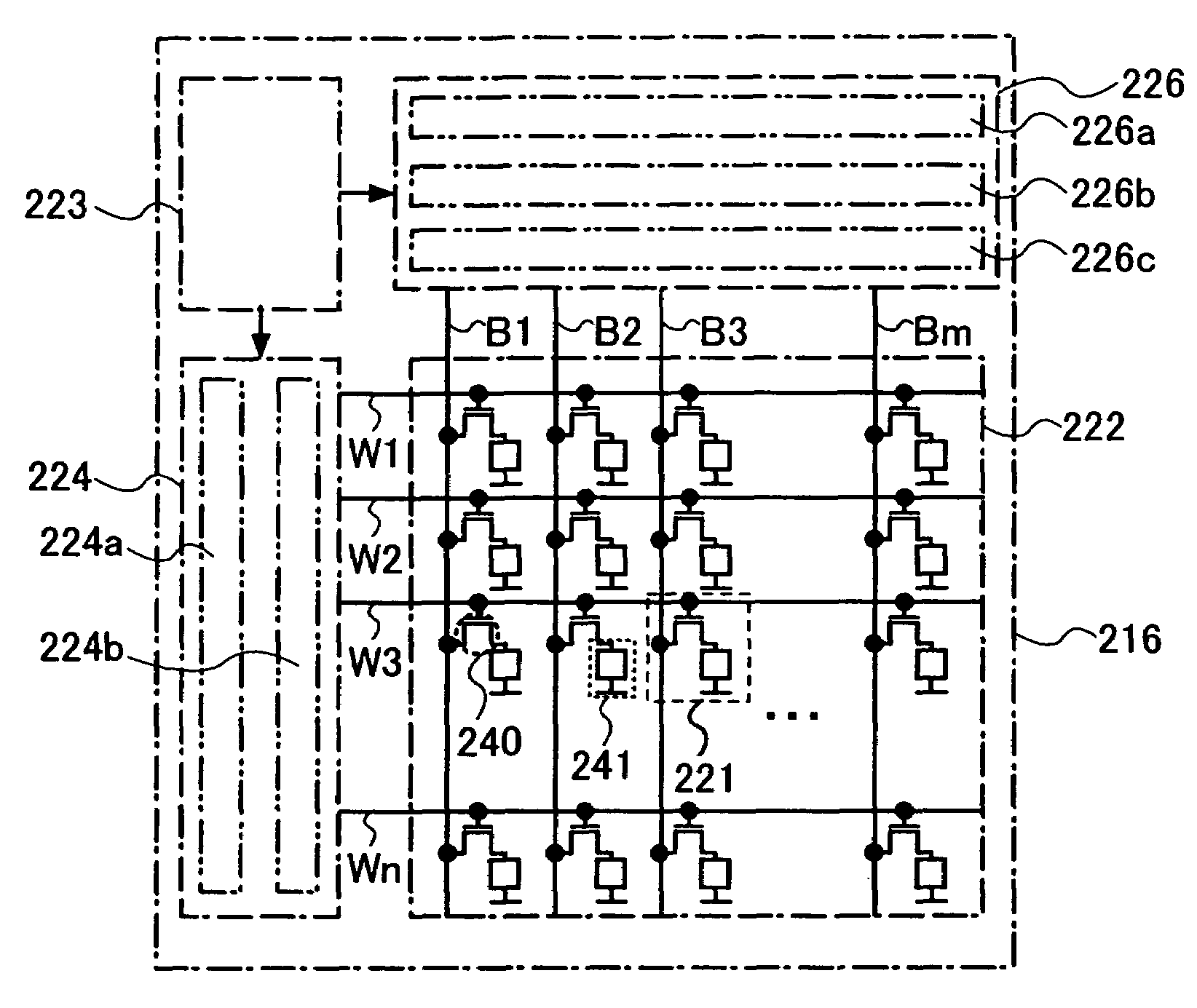
[0098]This embodiment mode will describe a storage circuit and a semiconductor device having a structure different from the structure shown in Embodiment Mode 2. Specifically, this embodiment mode will show a case of a storage circuit having an active matrix structure.

[0099]FIG. 8A shows a structural example of an organic memory shown in this embodiment mode, which includes a memory cell array 222 in which memory cells 221 are arranged in a matrix form; a bit line driver circuit 226 having a column decoder 226a, a reading circuit 226b, and a selector 226c; a word line driver circuit 224 having a row decoder 224a and a level shifter 224b; and an interface 223 having a writing circuit and the like to communicate with the outside. The structure of the storage circuit 216 shown here is just one example and the storage circuit 216 may further include other circuits such as a sense amplifier, an output circuit, and a buffer, and the writing circuit may be provided in the bit line driver c...


PUM


Abstract

An object of the present invention is to provide nonvolatile, rewritable, easily-manufactured, and inexpensive storage element, storage device, and semiconductor device, which are superior in switching characteristics and which has low operation voltage. In an element including a first conductive layer, a second conductive layer facing the first conductive layer, and a layer containing at least one kind of an organic compound provided between the first conductive layer and the second conductive layer, the organic compound can be electrochemically doped or dedoped. By feeding current in this element, the organic compound provided between the conductive layers is electrochemically doped, i.e., electrons are transported, whereby the conductivity can be increased by about three to ten digits.

Description

BACKGROUND OF THE INVENTION[0001]1. Field of Invention[0002]The present invention relates to a semiconductor device and particularly relates to a semiconductor device capable of storing, erasing, and rewriting data by using an organic compound for a storage circuit. Moreover, the present invention relates to a storage circuit (storage device) capable of storing, erasing, and rewriting data by using an organic compound.[0003]2. Description of the Related Art[0004]In recent years, identification technology where an ID (identification number) is assigned to each object so as to reveal data on the object such as history thereof has been attracting attention, which is utilized for production, management, and the like. Above all, semiconductor devices capable of sending and receiving data without contact have been developed. As such semiconductor devices, in particular, an RFID (Radio Frequency Identification) tag (also called an ID tag, an IC tag, an IC chip, an RF (Radio Frequency) tag,...

Claims


Application Information

Patent Timeline
Patent Type & Authority Patents(United States)
IPC IPC(8): G11C11/00
CPCB82Y10/00G11C13/0009G11C13/0014G11C13/0016H01L27/285H01L51/0591H10K19/202H10K10/50
Inventor NOMURA, RYOJI
Owner SEMICON ENERGY LAB CO LTD
Why Eureka
Try Eureka