Image sensor having a partial light-shielding layer and method for fabricating the same

a technology of image sensor and light shielding layer, which is applied in the field of image sensor, can solve the problems of high process cost, high driving voltage, and additional circuits, and achieve the effect of excellent display quality and optimal effective ratio

Inactive Publication Date: 2010-02-23
DONGBU ELECTRONICS CO LTD
View PDF15 Cites 10 Cited by
  • Summary
  • Abstract
  • Description
  • Claims
  • Application Information

AI Technical Summary

Benefits of technology

[0015]Another object of the present invention is to provide an image sensor and a method for fabricating the same in which the permeation position of red colored light, green colored light and blue colored light coincides with one another within a depletion area of a semiconductor substrate to obtain an optimal effective ratio from respective optical charges and the uniform quantity of the respective optical charges can be transferred / discharged to an interpolation circuit by signal processing transistors, thereby effectively displaying color images having excellent display quality (in color and resolution) approximate to a ratio of 1:1:1 with red, green and blue.

Problems solved by technology

However, the CCD has several drawbacks in that a high driving voltage is required, an additional circuit is required, and the process cost is high.
For this reason, the color images finally obtained by the interpolation circuit do not have a normal ratio of 1:1:1 with red, green and blue, thereby causing low display quality in color and resolution.

Method used


Image

  • Image sensor having a partial light-shielding layer and method for fabricating the same
  • Image sensor having a partial light-shielding layer and method for fabricating the same
  • Image sensor having a partial light-shielding layer and method for fabricating the same

Examples


Embodiment Construction

[0030]Reference will now be made in detail to the preferred embodiments of the present invention, examples of which are illustrated in the accompanying drawings. Wherever possible, the same reference numbers will be used throughout the drawings to refer to the same or like parts.

[0031]Hereinafter, an image sensor according to the present invention and a method for fabricating the same will be described as follows.

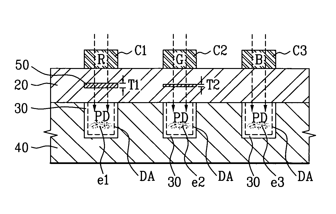
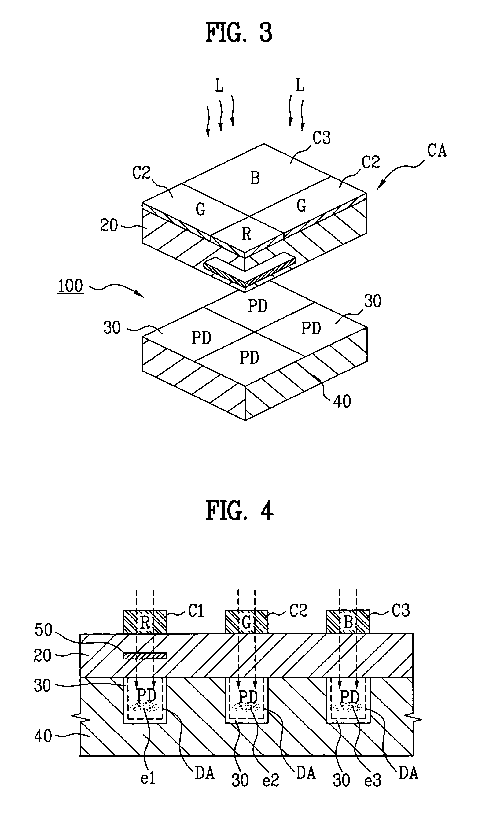
[0032]As shown in FIG. 3, a CMOS image sensor 100 of the present invention, i.e., a CMOS image sensor for displaying color images includes photodiodes 30 formed on a semiconductor substrate 40, generating and storing a series of optical charges from externally input lights L, and a color filter array CA coloring the externally input lights and transferring the colored lights to the photodiodes 30. In this case, an intermediate layer 20 is interposed between the color filter array CA and the photodiodes 30 so as to transfer the lights, which have transmitted the color filter...


PUM


Abstract

An image sensor and a method for fabricating the same are disclosed, in which a partial light-shielding layer is additionally arranged on a path of a particular colored light, for example, a red colored light that may cause excessive permeation, to partially shield the corresponding red colored light in a state that red colored light, green colored light and blue colored light are permeated into each photodiode of a semiconductor substrate, so that the permeation position of the red colored light coincides with that of the green colored light and the blue colored light each having the wavelength shorter than that of the red colored light, thereby normally generating optical charges caused by the red colored light in an effective depletion area of the photodiode like those caused by the green colored light and the blue colored light. The permeation position of a red colored light, a green colored light and a blue colored light coincides with one another within a depletion area of a semiconductor substrate to obtain an optimal effective ratio from respective optical charges and the uniform quantity of the respective optical charges can be transferred / discharged to an interpolation circuit by signal processing transistors, thereby effectively displaying color images having excellent display quality (in color and resolution) approximate to a ratio of 1:1:1 with red, green and blue.

Description

[0001]This application claims the benefit of the Korean Application No. P2003-101702 filed on Dec. 31, 2003, which is hereby incorporated by reference.BACKGROUND OF THE INVENTION[0002]1. Field of the Invention[0003]The present invention relates to an image sensor, and more particularly, to an image sensor and a method for fabricating the same in which a partial light-shielding layer is additionally arranged on a path of a particular colored light, for example, a red colored light that may cause excessive permeation, to partially shield the corresponding red colored light in a state that a red colored light, a green colored light, and a blue colored light are permeated into each photodiode of a semiconductor substrate, so that the permeation position of the red colored light coincides with that of the green colored light and the blue colored light each having the wavelength shorter than that of the red colored light, thereby normally generating optical charges caused by the red color...

Claims


Application Information

Patent Timeline
Patent Type & Authority Patents(United States)
IPC IPC(8): H04N3/14H01L31/062H04N5/225H01L27/146H01L27/14H01L31/10H04N1/46H04N5/335H04N5/369H04N5/374H04N9/04
CPCH01L27/14621H01L27/14623H01L27/14685H04N9/045H01L27/14645H04N2209/045H01L27/146H01L31/10
Inventor HAN, CHANG HUN
Owner DONGBU ELECTRONICS CO LTD
Why Eureka
Try Eureka