Scanning microscopy

a scanning microscopy and scanning technology, applied in the field of scanning microscopy, can solve the problems of relatively time-consuming scanning process and scan time, and achieve the effect of not negatively affecting each other

Active Publication Date: 2010-03-23
APPL MATERIALS ISRAEL LTD
View PDF19 Cites 10 Cited by
  • Summary
  • Abstract
  • Description
  • Claims
  • Application Information

AI Technical Summary

Benefits of technology

[0014]In embodiments of the present invention, a scanning microscope comprises an element, typically an acousto-optic (AO) element, which generates a multiplicity of traveling beams. The traveling beams are focused to spots at a surface being inspected, and returning radiation from the surface is imaged and detected at an array of detectors. The characteristics of the image may be improved by introducing one or more image enhancing elements into the optics irradiation and collection path.
[0016]The slit is aligned parallel with the traveling direction of the spots, and with the detectors, and dimensions of the slit and its position are set so that in a direction orthogonal to the slit, confocal effects are introduced, whereas in the slit direction, normal imaging takes place. Introduction of a one-dimensional slit reduces depth discrimination while relaxing the auto-focus requirements of the system, compared to a confocal two-dimensional circular aperture.
[0017]In an alternative embodiment, the image enhancing element comprises a Wollaston, Nomarski, or equivalent prism followed by an analyzer. The prism divides each of the traveling beams into two orthogonally polarized traveling beams, the beams being angularly displaced one from the other. The two beams are focused onto the surface being inspected, and the returning radiation is combined in the analyzer before being focused onto the detectors. Phase information of the surface is thus converted into different intensity levels at the detectors, and the different intensity levels enhance the visibility of aspects of the surface such as edges.
[0019]In other disclosed embodiments of the present invention, two or more of the enhancing elements described above are incorporated into one scanning microscope. The advantages of each of the different enhancing elements are incorporated into the one microscope, without negatively affecting each other.

Problems solved by technology

The scanning process is relatively time-consuming, and methods for reducing the scanning time, while maintaining the quality of the received signals, are well known in the semiconductor art.

Method used


Image

  • Scanning microscopy
  • Scanning microscopy
  • Scanning microscopy

Examples


Embodiment Construction

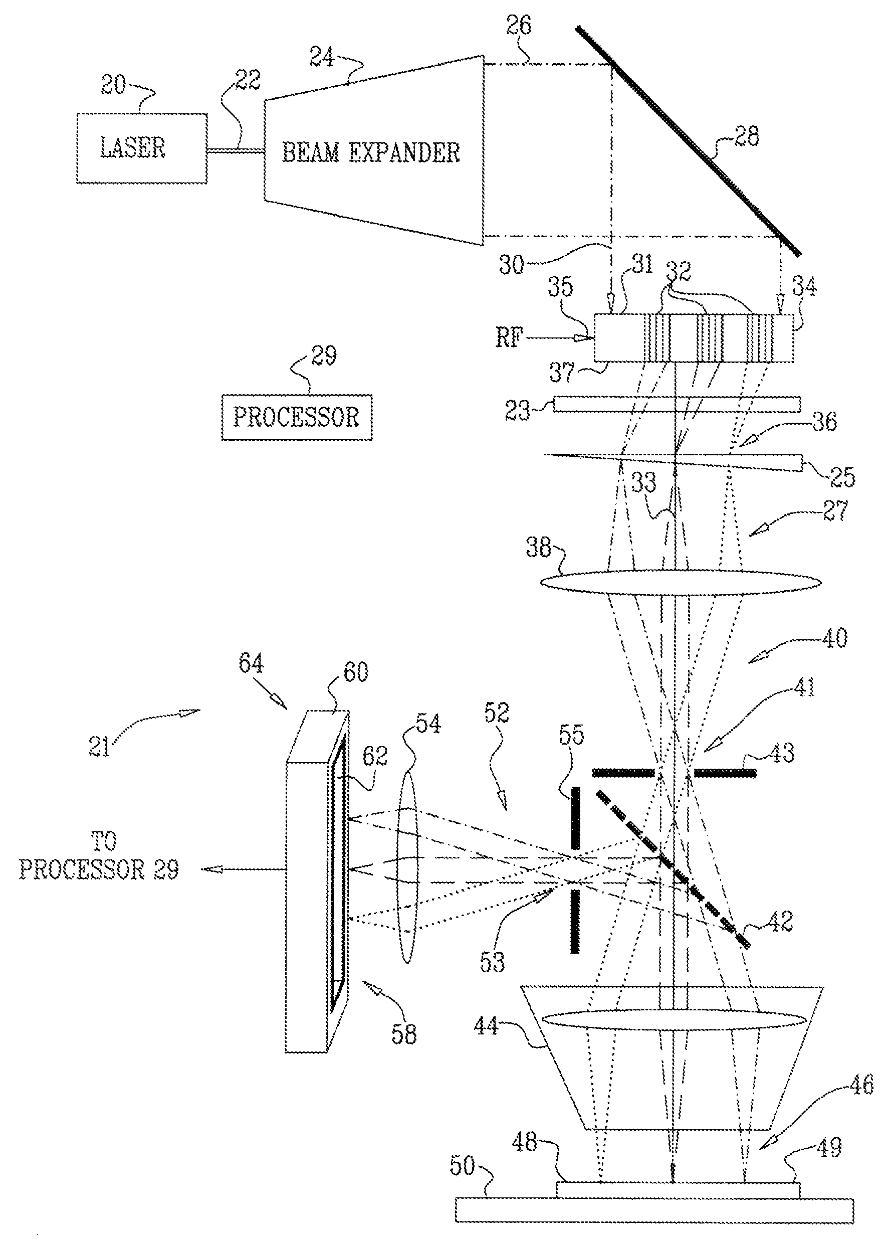
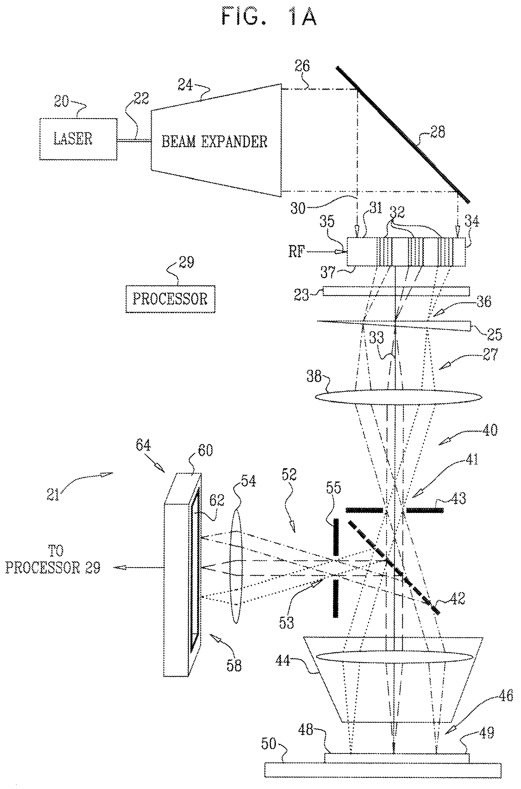
[0027]Reference is now made to FIG. 1A, which is a schematic diagram of a scanning microscope 21, and to FIG. 1B, which is a schematic side view of elements of the microscope, according to an embodiment of the present invention. Microscope 21 comprises a laser 20 which radiates a beam of coherent radiation 22 to a beam expander 24. Typically, laser 20 is selected to emit optical radiation at a wavelength in a region of the electromagnetic spectrum between and including far infra-red and deep ultra-violet (DUV), although it will be understood that the principles of the present invention apply equally to other wavelengths of the spectrum. Beam expander 24 generates an expanded collimated radiation beam 26 which reflects from a plane mirror 28 as a collimated radiation beam 30. A processor 29 operates elements of scanning microscope 21.

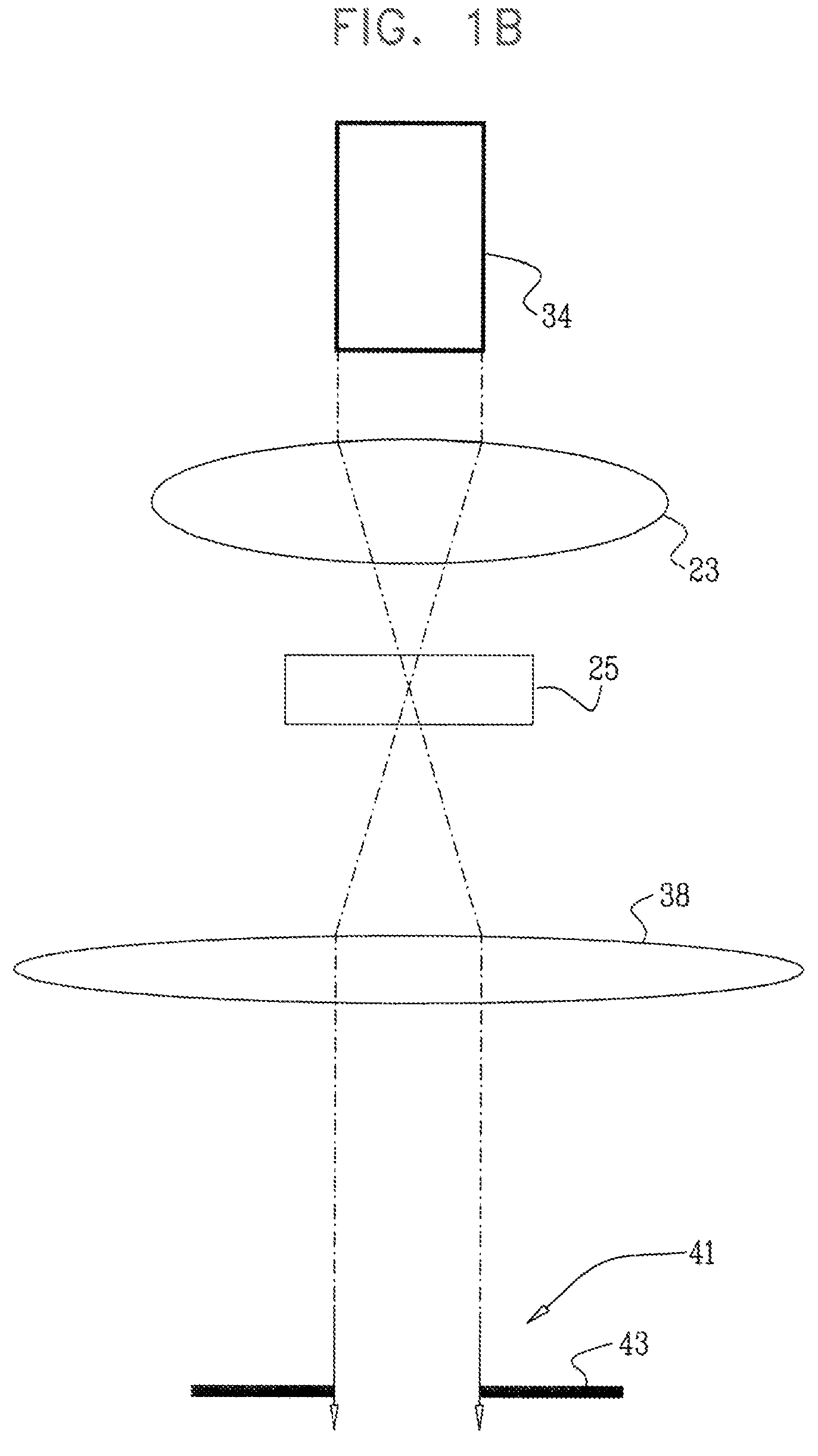
[0028]An acousto-optic (AO) element 34 receives beam 30 at a first surface 31 of the AO element, the first surface acting as a radiation input surface. ...


PUM


Abstract

Apparatus for imaging a surface, including scanning optics, which are configured to scan and focus one or more traveling beams onto the surface so as to form one or more traveling spots thereon. The apparatus also includes collection optics, which are arranged to collect radiation scattered from the one or more traveling spots and to focus the radiation to form one or more image spots traveling along a line. The apparatus also has a detecting assembly, which consists of a detector which is configured to generate a signal in response to the one or more traveling image spots, and a detector entry port interposed between the collection optics and the detector, which is coincident with the line. The apparatus also includes phase and / or polarization altering elements for the traveling beams.

Description

CROSS REFERENCE TO RELATED APPLICATIONS[0001]This application claims the benefit of U.S. Provisional Patent Application 60 / 736,983, filed Nov. 15, 2005, U.S. Provisional Patent Application 60 / 736,645, filed Nov. 15, 2005 and U.S. Provisional Patent Application 60 / 736,646, filed Nov. 15, 2005, which is are incorporated herein by reference.FIELD OF THE INVENTION[0002]The present invention relates generally to imaging an object, and specifically to imaging the object by scanning it with one or more sources of radiation, typically for the purpose of wafer and / or mask inspection.BACKGROUND OF THE INVENTION[0003]In production of a semiconductor die, imaging of the wafer upon which the dice are formed is an integral part of the fabrication process, and images are typically generated for many stages of the fabrication process. Typically, the wafer images are used for the purpose of inspection and / or quality control of the specific stages. One of the methods used to produce the images is to ...

Claims


Application Information

Patent Timeline
Patent Type & Authority Patents(United States)
IPC IPC(8): G01B11/02
CPCG01N21/21G01N21/47G01N21/95623G01N2021/4709G01N2021/4792
Inventor MESHULACH, DORONFELDMAN, HAIM
Owner APPL MATERIALS ISRAEL LTD
Why Eureka
Try Eureka