Optical amplifier-integrated super luminescent diode and external cavity laser using the same

a luminescent diode and optical amplifier technology, applied in the direction of lasers, semiconductor amplifier structures, semiconductor lasers, etc., can solve the problems of wlfp-ld and rsoa modulation structures, limited data rates of 1.25 gb/s for direct modulation, and not suitable for wdm-passive optical networks (pon)

Inactive Publication Date: 2010-03-30
ELECTRONICS & TELECOMM RES INST
View PDF1 Cites 12 Cited by
  • Summary
  • Abstract
  • Description
  • Claims
  • Application Information

AI Technical Summary

Problems solved by technology

A re-modulation structure employing the WLFP-LD and the RSOA has disadvantages of being dependent upon properties of the light source and being limited to a data rate of 1.25 Gb / s for direct modulation.
Even though such an SLD may have a reduced reflectance of the output facet, it is not suitable for a WDM-passive optical network (PON) due to increase in threshold current and operation current.
Such an SLD is inappropriate for a PLC-ECL and particularly a PLC-ECL for a WDM-PON because of its overly high threshold current.

Method used


Image

  • Optical amplifier-integrated super luminescent diode and external cavity laser using the same
  • Optical amplifier-integrated super luminescent diode and external cavity laser using the same
  • Optical amplifier-integrated super luminescent diode and external cavity laser using the same

Examples


Embodiment Construction

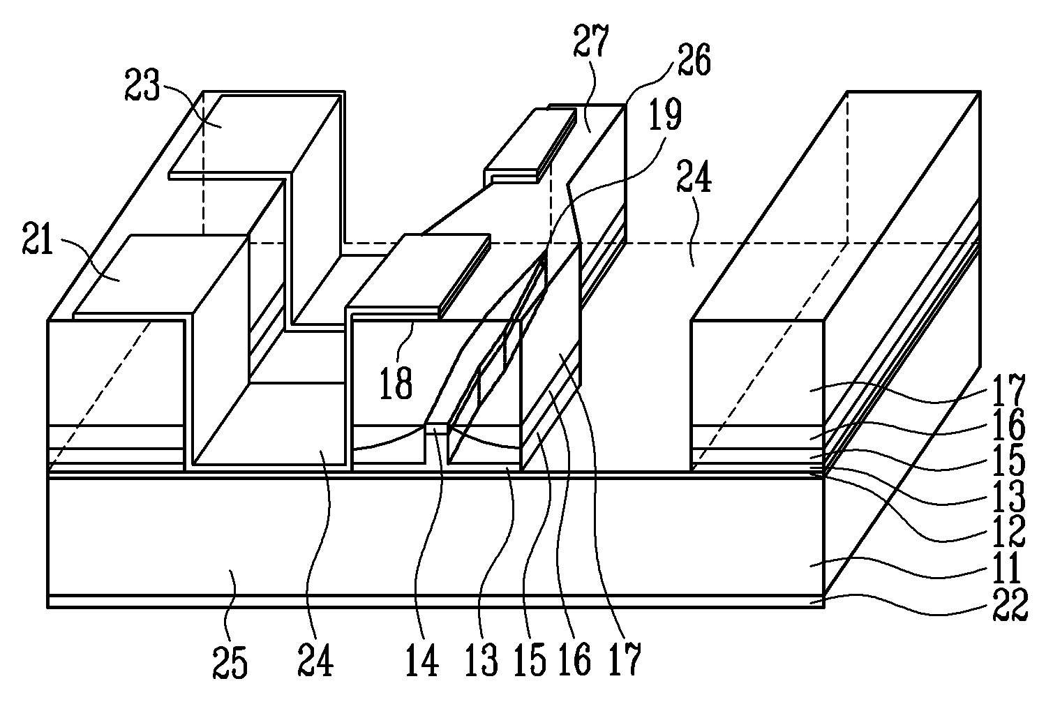
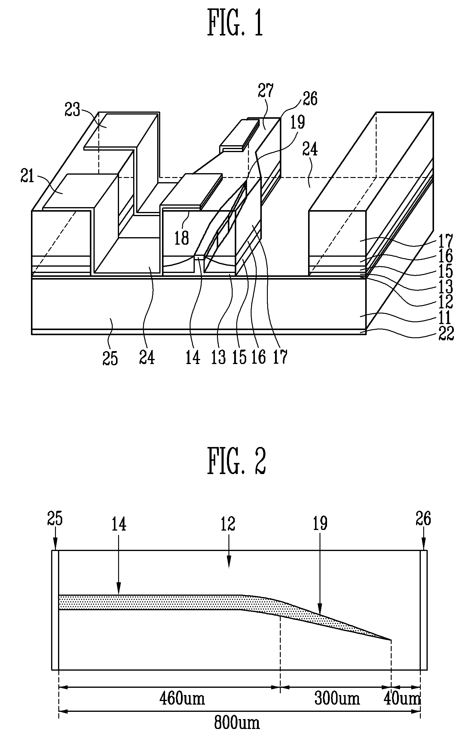
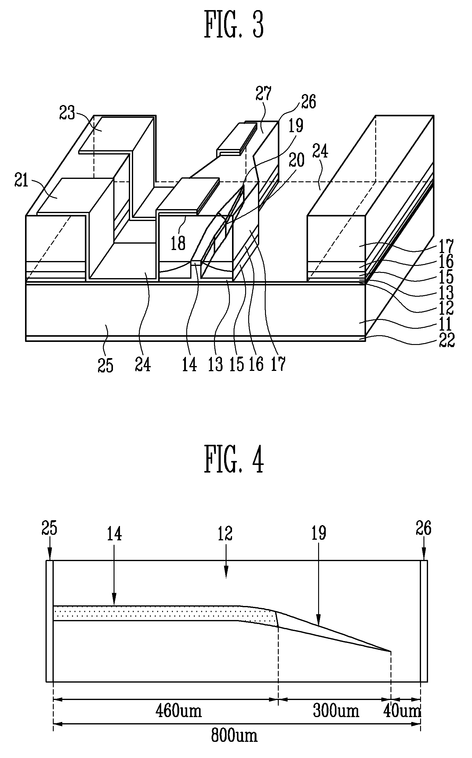
[0031]Hereinafter, exemplary embodiments of the present invention will be described in detail with reference to the accompanying drawings. The exemplary embodiments can be modified in various ways and are not intended to determine the scope of the present invention, but rather to enable those skilled in the art to embody and practice the present invention. The drawings are not necessarily to scale, emphasis instead being placed on illustrating the principles of the invention. Like elements are denoted by like reference numerals throughout.

[0032]An active layer of a super luminescent diode (SLD), which is used in a Wavelength Divisional Multiplexing passive optical network (WDM-PON) optical line terminal (OLT) and an optical network unit (ONU), and an active layer of a semiconductor optical amplifier (SOA) have the same structure of a growth layer and an optical waveguide except that the former has a structure of polarization-sensitive, compressive strain-compensated multiple quantum...


PUM


Abstract

Provided is a super luminescent diode having low power consumption due to low threshold current and a high output power in low-current operation, which is suitable for an external cavity laser. The super luminescent diode for use in the external cavity laser is divided into a super luminescent diode (SLD) region and a semiconductor optical amplifier (SOA) region to provide a light source having a low threshold current and a nearly double output power of a conventional SLD.A super luminescent diode-integrated reflective optical amplifier includes a substrate that has a super luminescent diode (SLD) region and a semiconductor optical amplifier (SOA) region for amplifying light generated from the SLD region, an optical waveguide that has a buried heterostructure, the buried heterostructure including an active layer extending over the SLD and SOA regions on the substrate and tapered in the SOA region; a current blocking layer formed around the active layer for blocking a current flow to layers other than the active layer, the current blocking layer including a stack of semiconductor layers having different conductivity types; and a clad layer formed on the optical waveguide and the current blocking layer.

Description

CROSS-REFERENCE TO RELATED APPLICATION[0001]This application claims priority to and the benefit of Korean Patent Application No. 2007-133553, filed Dec. 18, 2007, the disclosure of which is incorporated herein by reference in its entirety.BACKGROUND[0002]1. Field of the Invention[0003]The present invention relates to a super luminescent diode, and more particularly, to a 2-section super luminescent diode in which a super luminescent diode and an optical amplifier are formed as a single platform.[0004]This work was supported by the IT R&D program of MIC / IITA [2006-S-073-02, Nano flexible opto-electric PCB module for portable display].[0005]2. Discussion of Related Art[0006]To construct a cost-effective Wavelength Division Multiplexing (WDM) subscriber network system, it is essential to develop a stable and cost-effective light source. Particularly, as every subscriber in the WDM subscriber network system is assigned a specific wavelength for communication, it is necessary to have a w...

Claims


Application Information

Patent Timeline
Patent Type & Authority Patents(United States)
IPC IPC(8): H01S3/00H01S5/00H01L33/00H01L33/06H01L33/10H01L33/12H01L33/38H01L33/46H01S5/026H01S5/50
CPCH01L33/0045H01S5/026H01S5/141H01S5/50H01S5/101H01S5/1014H01S5/16H01S5/227H01S5/30
Inventor OH, SU HWANJU, JUNG JIN
Owner ELECTRONICS & TELECOMM RES INST
Why Eureka
Try Eureka