Three-axis inertial sensor and method of forming

a three-axis inertial sensor and sensor technology, applied in the direction of speed/acceleration/shock measurement, acceleration measurement in multiple dimensions, instruments, etc., can solve the problems of small sensor size, low sensitivity of bulk micromachined sensor, and large sensor siz

Inactive Publication Date: 2010-04-06
EVIGIA SYST
View PDF2 Cites 40 Cited by
  • Summary
  • Abstract
  • Description
  • Claims
  • Application Information

AI Technical Summary

Problems solved by technology

While exhibiting high sensitivity, such sensors are relatively large in size.
Since film thicknesses are typically limited, the sensors can be relatively small, though generally exhibiting lower sensitivity than bulk micromachined sensors due to a smaller proof mass.

Method used


Image

  • Three-axis inertial sensor and method of forming
  • Three-axis inertial sensor and method of forming
  • Three-axis inertial sensor and method of forming

Examples


Embodiment Construction

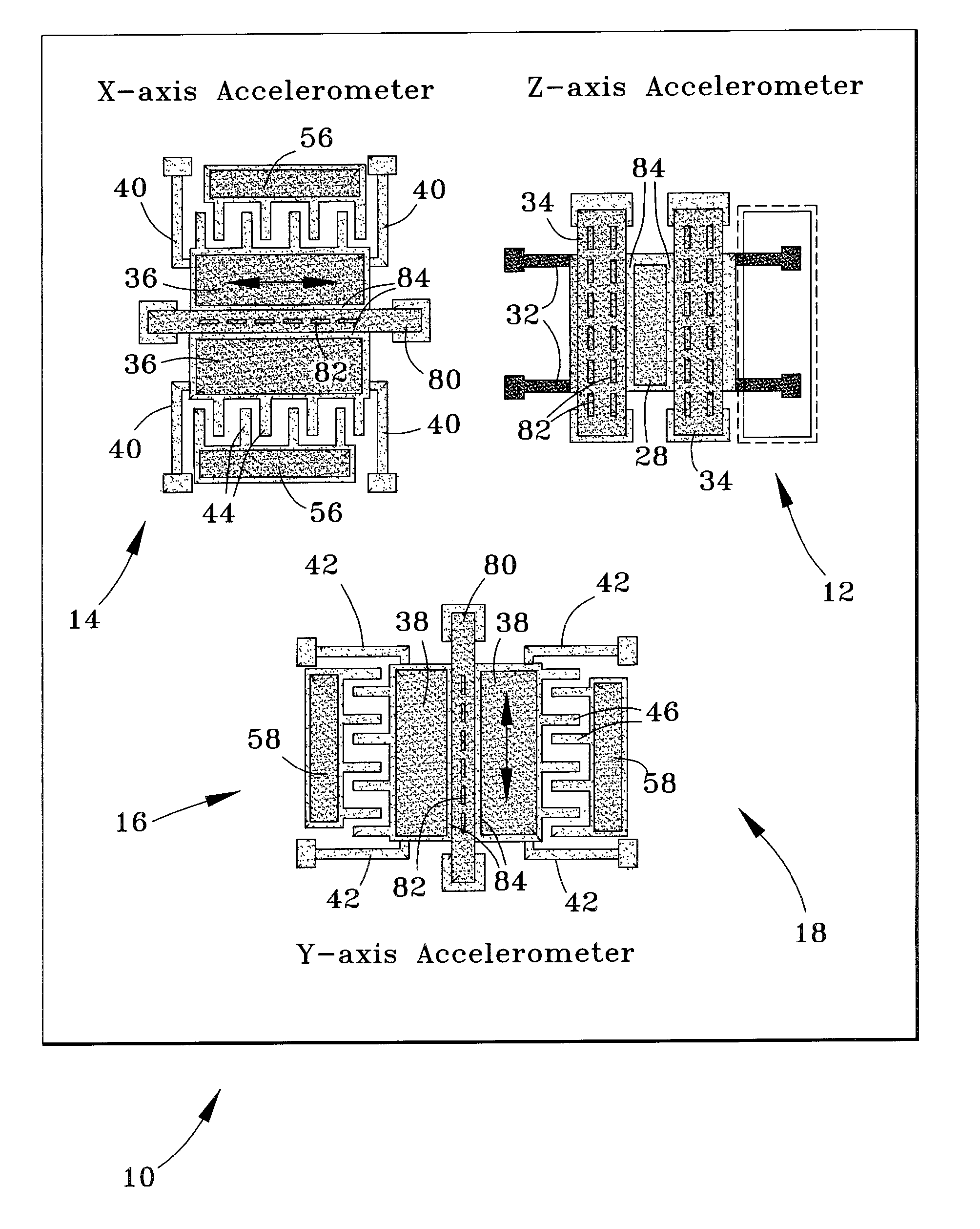
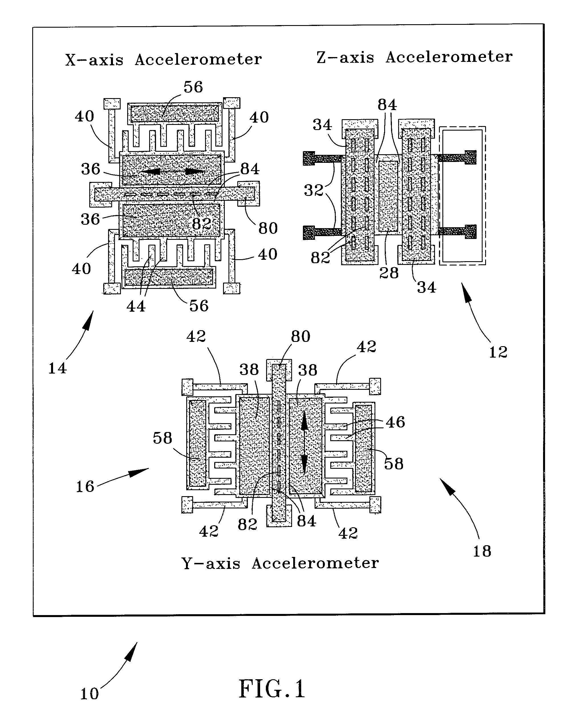
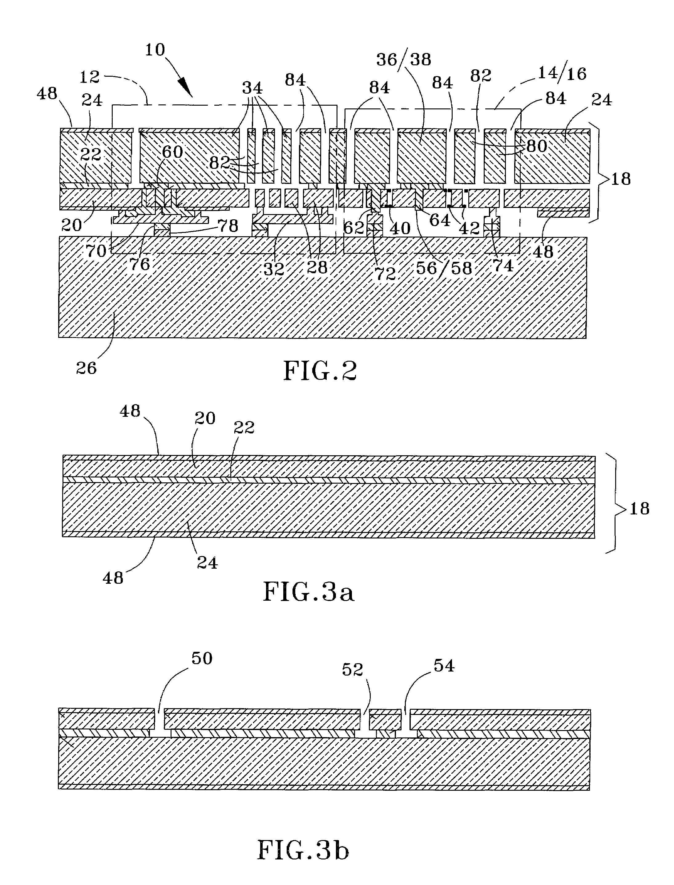
[0018]FIG. 1 schematically represents a plan view of a three-axis inertial sensor chip 10 containing z-axis, x-axis, and y-axis inertial sensing devices 12, 14 and 16, respectively, all of which are formed with the use of an SOI wafer (18 in FIGS. 2 and 3a through 3l) bonded to substrate 26 (FIGS. 2, 3k, and 3l). The substrate 26 may be formed of glass or a semiconductor material, but is preferably a silicon wafer fabricated to contain an integrated circuit, more preferably a silicon wafer with CMOS circuitry (hereinafter, a CMOS wafer 26). As is conventional, the SOI wafer 18 is shown in FIGS. 2 and 3a through 3l as including an electrically-conductive (e.g., doped silicon) device layer 20 separated from an electrically-conductive (e.g., doped silicon) handle layer 24 by an electrically-insulative buried oxide (BOX) layer 22. While the SOI wafer 18 is preferred, it will become evident to those skilled in the art that other materials and processes could be employed to fabricate a th...


PUM

PropertyMeasurementUnit
conductiveaaaaaaaaaa
massaaaaaaaaaa
electricallyaaaaaaaaaa

Abstract

A three-axis inertial sensor and a process for its fabrication using an silicon-on-oxide (SOI) wafer as a starting material. The SOI wafer has a first conductive layer separated from a second conductive layer by an insulative buried oxide (BOX) layer. The SOI wafer is fabricated to partially define in its first conductive layer at least portions of proof masses for z, x, and y-axis sensing devices of the sensor. After a conductive deposited layer is deposited and patterned to form a suspension spring for the proof mass of the z-axis sensing device, the SOI wafer is bonded to a substrate that preferably carries interface circuitry for the z, x, and y-axis devices, with the SOI wafer being oriented so that its first conductive layer faces the substrate. Portions of the BOX layer are then etched to fully release the proof masses.

Description

CROSS REFERENCE TO RELATED APPLICATIONS[0001]This application claims the benefit of U.S. Provisional Application No. 60 / 841,429, filed Aug. 31, 2006, the contents of which are incorporated herein by reference.BACKGROUND OF THE INVENTION[0002]The present invention generally relates to motion sensing devices and their fabrication methods. More particularly, this invention relates to a three-axis inertial sensor and a process for its fabrication.[0003]Three-axis inertial sensors that respond to inertial forces in the x, y and z axes are finding applications in the detection of shock, vibration, and acceleration. These sensors have been fabricated with MEMS (micro-electro-mechanical systems) technology using bulk micromachining, surface machining, or a combination of the two. Particular interest in capacitive three-axis accelerometers has existed in part because they are capable of low power consumption and high sensitivity. Such sensors use the displacement of a proof mass in response ...

Claims


Application Information

Patent Timeline
Patent Type & Authority Patents(United States)
IPC IPC(8): G01P15/125H01L21/00
CPCG01P15/0802G01P15/125G01P15/18Y10T29/49117G01P2015/0814G01P2015/0828
Inventor GOGOI, BISHNU PRASANNAYAZDI, NAVID
Owner EVIGIA SYST
Why Eureka
Try Eureka