Electrical connection between cable and printed circuit board for high data speed and high signal frequency

a technology of high data speed and high signal frequency, applied in the direction of fixed connections, coupling device connections, printed circuit aspects, etc., can solve the problems of user suffering, data at the receiving endpoint of the connection is randomly distorted, data retransmission triggers, etc., to reduce decoupling, keep costs very low, and uniform connection impedance

Inactive Publication Date: 2010-04-06
CHEN HUBERT +1
View PDF2 Cites 61 Cited by
  • Summary
  • Abstract
  • Description
  • Claims
  • Application Information

AI Technical Summary

Benefits of technology

[0013]Once that the connection of the most critical electrical wires (usually high speed serial data line pairs with differential encoding) with the interconnection PCB have been completed properly, the invention here described allows to use traditional PCB routing techniques to reach the target PCB. The Interconnection PCB is then kept in place by a proper retention mechanism and connects to the target PCB by soldering (galvanic connection) the Interconnection PCB to the target PCB (“PCB edge solder connector”). Alternatively the interconnection PCB can become a connector by means of a molding process or directly soldering it to a traditional connector. The Intermediate PCB can attach to the Target PCB even by other means that are alternative implementation of the presented invention. Also, the Intermediate PCB can be the Target PCB. The Interconnection PCB can be made as simple as a thin two layers PCB having one layer as reference ground and the second layer as impedance matched and length balanced traces. The possibility to use a simple dual layer thin PCB allows to keep cost very low. Considering all the added advantages described in details in the following paragraphs, it is believed that the added cost due to the introduction of the Interconnection PCB is very well absorbed by the overall advantages and savings that this solution enables to the process.
[0014]The proposed solution is supported by a proper arrangement of the wires as the electrical wires in a flat section shape electrical cable, instead of the usual round section. The Interconnection PCB is designed in a way that individual wire solder pads are perfectly aligned with the arrangement of the wire in the flat cable. This layout and arrangement by itself removes the problem to rearrange each cable wire to its solder point, while also removing any possibility of mistake in the soldering order. In addition, both shielding braids and drain wires are properly collected and well kept in place with conductive gluing Copper Tape and soldered to the respective grounds: Shield Ground and Digital Ground. Advantages from mechanical, electrical, manufacturing and functional perspectives are several and evident: Extreme control over length balancing of each electrical wire with realistic possibility to reach precision of + / −0.1 mm, very reduced decoupling between wire and it's reference ground (in the range of 1 mm) with consequent advantage for a very uniform connection impedance, very easy visual inspectionability of each connection, very thin global assembly of the connection (less than 5 mm of thickness) with obvious mechanical advantages for the final application, higher reliability, higher automatization of the manufacturing process, resulting in a total cost reduction and higher quality.
[0015]Improving the mechanical placement of the cable and of the individual electrical wires ensures the following advantages at electrical and quality level of the transmitted signal: Low jitter, low electromagnetic interference (EMI) irradiated, very low impedance discontinuity (both time and space wise), very low impedance variation (Delta) over all the connection, return ground wires remain very close to the referenced signal wire, ensuring low EMI emission and low sensibility to external electromagnetic fields. Each of these advantages individually increases the quality of the transmission channel, granting signal integrity and simplifying the design of systems and circuits having transfer speeds of 2.5 Gbps or more.
[0016]The final result is a very solid and reliable connection between the cable and the final PCB, with the most perfect electrical impedance continuity.

Problems solved by technology

Such reflections add up to the electrical waveform of signal itself, causing random errors in the data at the receiving endpoint of the connection.
The errors are usually detected by complex error detection and correction algorithms, that can trigger data retransmissions.
Ultimately the user suffers, depending on the nature of the data delivered, a slower transmission line or, in case of real time audio / video transmissions, less overall perceived quality.
These EMI not only create an unwanted effect that has to be minimized to safeguard EMI pollution and to obey to national and international standards such as FCC and CE, but also subtract energy for the meaningful signal, making it more weak and subject to additional vulnerability to the above mentioned negative effects.
It is also common experience that the greater the speed and frequency of data is involved, the more the connector is getting sophisticated, cumbersome, complex, expensive.
With the progressive increase of the data transfer speeds and the reduction in the mechanical dimensions of the interconnections, being able to produce connectors meeting market needs will be more and more difficult for connectors and cables manufacturers, also taking into account that there is a consistent manual labor involved in the process.
Alternatively, the standards that create the foundations of signal protocols can take into account a specific amount of impedance discontinuity and compensate it, at the cost of some less performance and efficiency.
Instead it is already a big challenge to meet from the view point of a cable maker.
The simple fact to have to spread the wires of a cable to the connector solder points requires that some of the wires follow a longer path than others and therefore ensuring that the cable length difference, among several scattered wires, is less than 1 mm becomes an almost impossible task.
To make things worse, as usually cables have one connector at each end, the errors at each end can in the worst case add up, so then having a total length difference below 2 mm (1 mm at each side) is almost impossible to control.
All these precision levels cannot be verified by a visual control and test devices that can perform an automated / numeric verification are very expensive and most of the time not affordable to the vast majority of cable makers, especially since cables are seen as commodities with limited added value.
From all the above description it is clear how critical and complex it is to ensure the high standard levels required for manufacturing impedance matched cables when featuring connectors at their ends.

Method used


Image

  • Electrical connection between cable and printed circuit board for high data speed and high signal frequency
  • Electrical connection between cable and printed circuit board for high data speed and high signal frequency
  • Electrical connection between cable and printed circuit board for high data speed and high signal frequency

Examples


second embodiment

[0029]FIG. 3: shows a top view of the invention.

DESCRIPTION OF THE PREFERRED EMBODIMENTS

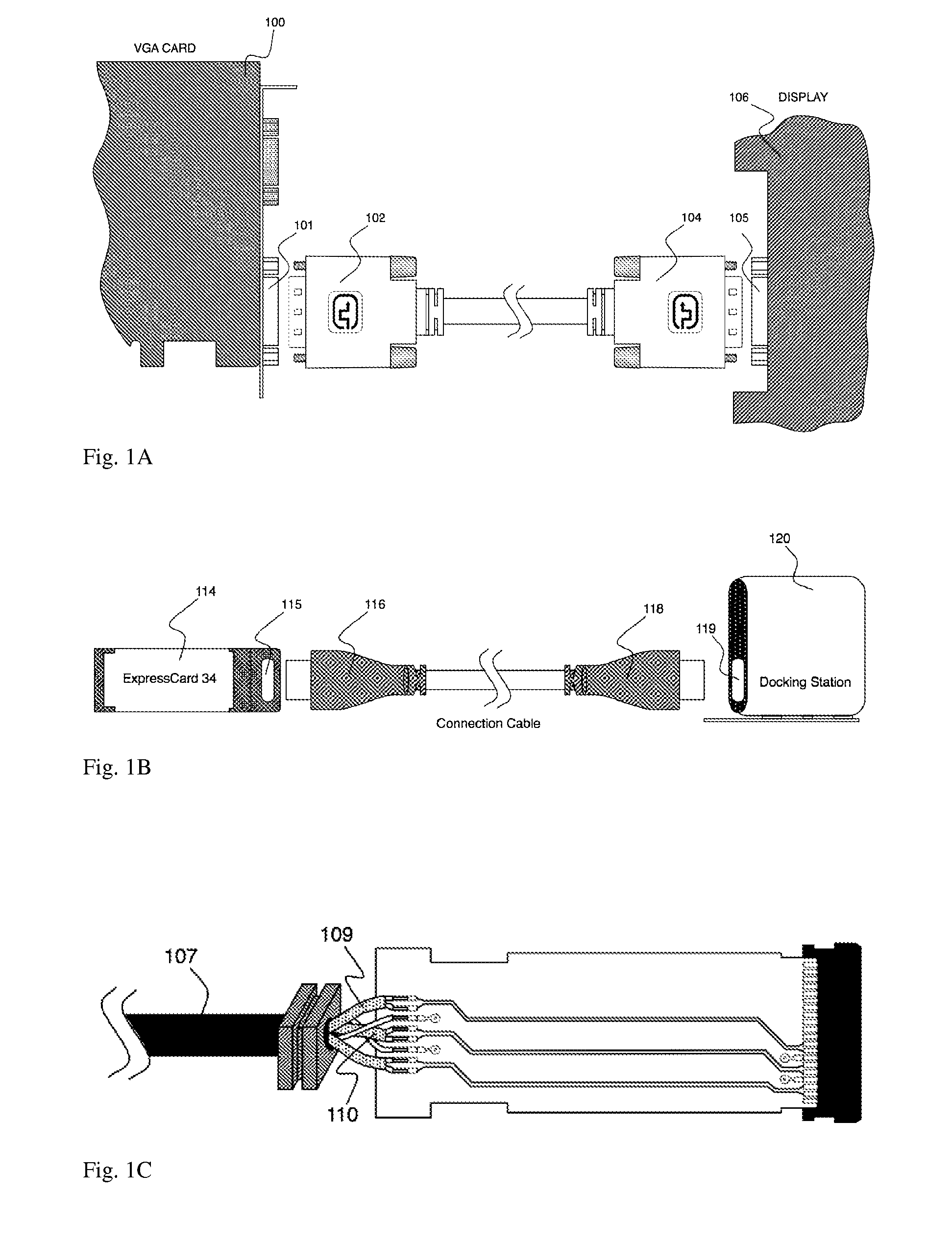
[0030]As already described above with reference to the prior art, and with reference to FIG. 1A and FIG. 1B, for the known solutions it is common practice to feature two connector pairs 101, 102, 104, 105 (FIG. 1A) 115, 116 and 118, 119 (FIG. 1B) placed in the connection between two electronic devices 100 and 106 (FIG. 1A), 114 and 120 (FIG. 1B), implying an interruption of the electrical impedance through the connection.

[0031]Removing the connectors (FIG. 1C) there is a severe inconvenience due to having individual wires of the cable 107 having different lengths, violating the rule of the balanced length of the high speed electrical connections 109 and 110, not to mention the differences in the bad ground coupling and shielding schemas.

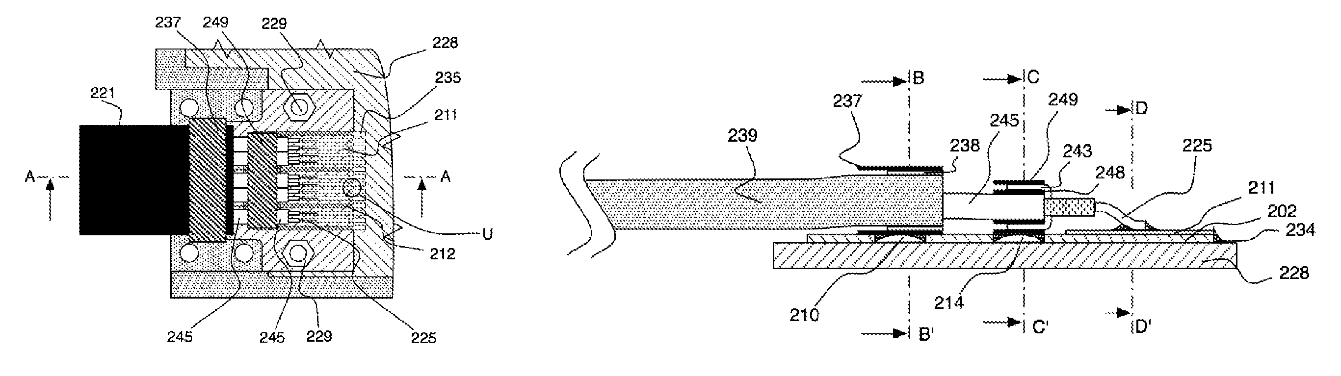
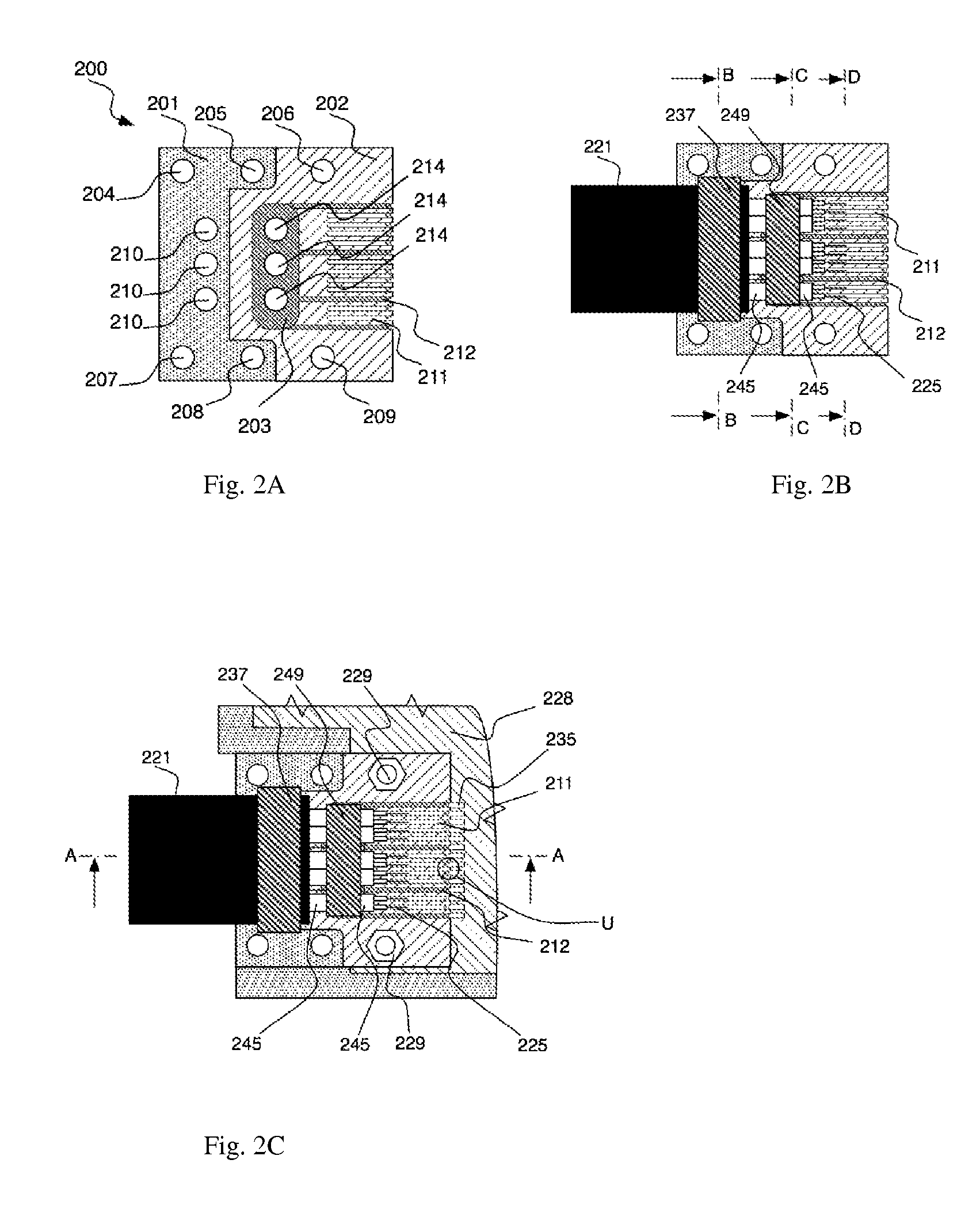
[0032]A detailed reference is now made to the preferred first embodiment of the present invention, as per FIGS. 2A trough 2J.

[0033]As generally known, cables used...


PUM


Abstract

A direct galvanic connection between a cable, having a preferred flat cross-section, and an electronic Printed Circuit Board (“Target PCB”) (228) by means of an intermediate PCB (“Interconnection PCB”) (200) allowing an impedance matched and length balanced electrical connection is described, thus offering ideal conditions for high speed and high frequency data connections. At the same time, the connection allows to keep the flexibility of a modular production and assembly workflow, typical of the use of well known connectors.

Description

DESCRIPTION OF THE INVENTION[0001]1. Field of the Invention[0002]The described invention relates in general to high speed electrical signal connections, involving connections between cables with specific impedance rating and impedance matched printed circuit board (PCB) traces, according to the preamble of claim 1.[0003]2. Background of the Invention[0004]The functionality of many modern electronic devices often requires interconnecting different components through cable or wire links that carry high speed digital data. A common example can be the usage of external hard disk drives connected with USB cables, or even the connection of displays (computer monitors or TVs) using DVI or HDMI digital video connections. Current trend in the industry is to keep increasing the signal frequency to reach higher speeds, and to use serial data transfer approach, that again involves higher speed / frequency of electrical signals, often propagated on two wires (a wire pair or multiple wire pairs to ...

Claims


Application Information

Patent Timeline
Patent Type & Authority Patents(United States)
IPC IPC(8): H01R12/00
CPCH01R9/038H01R12/62H05K1/0243H05K3/3405H01R43/0256H05K1/141H05K2203/0455H05K3/341H05K3/3442H05K2201/09181H05K2201/09809H05K2201/10356H01R13/65918
Inventor CHEN, HUBERTORLANDINI, ASCANIO
Owner CHEN HUBERT
Why Eureka
Try Eureka