Photomask blank and photomask

a technology of photomask and blank, applied in the field of photomask blank and photomask, can solve the problems of preventing effective pattern transfer, reducing the application range of photomask, so as to achieve high light shielding property and chemical stability, and high etching processability.

Active Publication Date: 2010-04-06
SHIN ETSU CHEM CO LTD +1
View PDF27 Cites 22 Cited by
  • Summary
  • Abstract
  • Description
  • Claims
  • Application Information

AI Technical Summary

Benefits of technology

[0032]In the invention, an antireflective film may be disposed on the light-shielding film. In one embodiment wherein the antireflective film is made of a transition metal silicide compound such as a transition metal silicide oxide, transition metal silicide nitride, transition metal silicide oxynitride, transition metal silicide oxycarbide, transition metal silicide carbonitride or transition metal silicide oxide nitride carbide, the light-shielding film and the antireflective film can be etched by fluorine dry etching, ensuring very high etching processability.
[0033]In another embodiment wherein the antireflective film is made of a chromium compound such as a chromium oxide, chromium nitride, chromium oxynitride, chromium oxycarbide, chromium carbonitride or chromium oxide nitride carbide, the light-shielding film and the antireflective film are such that they can be fully processed using a thin resist film. They can be processed without substantial damage to the resist, and the chemical stability during cleaning is satisfactory.BENEFITS OF THE INVENTION
[0034]The photomask blank having a light-shielding film as constructed according to the invention is a photomask blank having a light-shielding film possessing high light-shielding property and chemical stability, which can be etched or processed under sufficient etching conditions or within a sufficient etching time to minimize the damage to the resist during etching, even when the light-shielding film is overlaid with an antireflective film. Then the resist can be formed relatively thin, thereby avoiding the problems associated with an increase of resist film aspect ratio and enabling higher accuracy photomask pattern formation.

Problems solved by technology

In the recent semiconductor processing technology, a challenge to higher integration of large-scale integrated circuits places an increasing demand for miniaturization of circuit patterns.
As a result, the resist pattern profile is degraded, preventing effective pattern transfer, and in some cases, there occurs resist pattern collapse or stripping.
If etching is carried out through a thin resist film, accurate transfer of the resist pattern is difficult.
It is a task of some difficulty for the resist to have both a high resolution and etch resistance that allows for high accuracy etching.
All these metal silicide films have insufficient chemical stability to chemical cleaning as the final step of the photomask fabrication process, and particularly when the films are made thin, may lose the physical properties the film should maintain during the cleaning step.

Method used


Image

  • Photomask blank and photomask
  • Photomask blank and photomask
  • Photomask blank and photomask

Examples


example

[0070]Examples and Comparative Examples are given below for illustrating the invention although the invention is not limited thereto.

examples 6-12

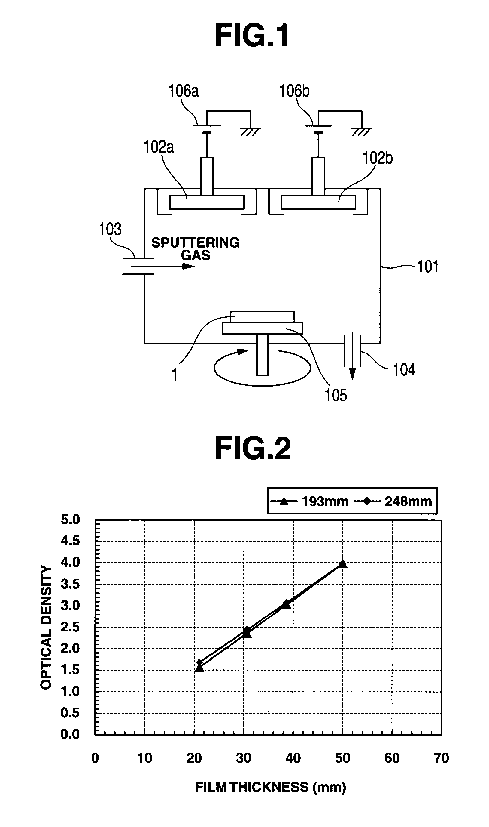
[0086]Photomask blanks (binary mask blanks) having a light-shielding film and an antireflective film deposited on a substrate were prepared by the following procedure.

[0087]Antireflective Film of Molybdenum Silicide Compound (Examples 6-9)

[0088]First, a light-shielding film (Si:Mo=9:1 in atomic ratio) having a thickness of 25 nm was deposited under the same conditions as in Example 1.

[0089]Next, using a DC sputtering apparatus having two targets as shown in FIG. 1, an antireflective film of molybdenum silicide nitride was deposited on the light-shielding film. Sputtering gases, Ar gas at a flow rate of 5 sccm, N2 gas at 50 sccm, and O2 gas at 0.2 sccm were introduced so as to establish a gas pressure of 0.1 Pa in the sputtering chamber. Two targets were used herein: a Mo target as the transition metal source and a Si (single crystal) target as the silicon source. Discharge powers of 150 W and 850 W were fed to the Mo and Si targets, respectively, while the substrate was rotated at 3...

example 13

[0105]A halftone phase shift mask blank was fabricated and then processed into a halftone phase shift mask as follows.

[0106]At the start, a first layer of 10 nm thick was deposited on a quartz substrate of 6 inch square by a sputtering deposition process, specifically by using a MoZrSi4 sintered body and a Si single crystal as sputtering targets, feeding a discharge power of 560 W and 1,000 W to the MoZrSi4 and Si targets, respectively, and rotating the substrate at 30 rpm. During the process, a gas mixture of 8 sccm of Ar, 20 sccm of N2, and 5 sccm of O2 was introduced as the sputtering gas. The gas pressure during sputtering was set at 0.15 Pa.

[0107]Then, a second layer of 40 nm thick as shown in Table 1 was deposited while changing the discharge powers so as to apply 430 W to the MoZrSi4 target and 1,000 W to the Si target, changing the sputtering gas to a gas mixture of 15 sccm of Ar, 100 sccm of N2, and 1 sccm of O2, rotating the substrate at 30 rpm, and setting a gas pressure ...


PUM

PropertyMeasurementUnit
optical densityaaaaaaaaaa
thicknessaaaaaaaaaa
thicknessaaaaaaaaaa

Abstract

A photomask blank to be used as a material for a photomask is provided with a mask pattern having a transparent area and an effectively opaque area to exposure light on a transparent substrate. On the transparent board, one or more layers of light shielding films are formed with or without other film (A) in between, at least one layer (B) which constitutes the light shielding film includes silicon and a transition metal as main component, and a molar ratio of silicon to the transition metal is silicon:metal=4-15:1 (atomic ratio). The photomask provided with the mask pattern having the transparent area and the effectively opaque area to exposure light on the transparent board is also provided.

Description

TECHNICAL FIELD[0001]This invention relates to photomask blanks and photomasks for use in the microfabrication of semiconductor integrated circuits, charge coupled devices (CCD), liquid crystal display (LCD) color filters, magnetic heads or the like.BACKGROUND ART[0002]In the recent semiconductor processing technology, a challenge to higher integration of large-scale integrated circuits places an increasing demand for miniaturization of circuit patterns. There are increasing demands for further reduction in size of circuit-constructing wiring patterns and for miniaturization of contact hole patterns for cell-constructing inter-layer connections. As a consequence, in the manufacture of circuit pattern-written photomasks for use in the photolithography of forming such wiring patterns and contact hole patterns, a technique capable of accurately writing finer circuit patterns is needed to meet the miniaturization demand.[0003]In order to form a higher accuracy photomask pattern on a pho...

Claims


Application Information

Patent Timeline
Patent Type & Authority Patents(United States)
IPC IPC(8): G03F1/00G03F1/32G03F1/68G03F1/80H01L21/027
CPCG03F1/14G03F1/68G03F1/58G03F1/46G03F1/38G03F1/50
Inventor YOSHIKAWA, HIROKIINAZUKI, YUKIOOKAZAKI, SATOSHIHARAGUCHI, TAKASHIIWAKATA, MASAHIDETAKAGI, MIKIOFUKUSHIMA, YUICHISAGA, TADASHI
Owner SHIN ETSU CHEM CO LTD
Why Eureka
Try Eureka