Method for improved growth of semipolar (Al,In,Ga,B)N

a growth method and semi-polar technology, applied in the direction of polycrystalline material growth, crystal growth process, chemically reactive gas, etc., can solve the problems of reduced oscillator strength, red-shifted emission, restricted carrier recombination efficiency, etc., to improve electrical, optical and device properties, improve layer properties, and reduce substrate symmetry

Active Publication Date: 2010-04-06
JAPAN SCI & TECH CORP
View PDF46 Cites 253 Cited by
  • Summary
  • Abstract
  • Description
  • Claims
  • Application Information

AI Technical Summary

Benefits of technology

[0041]The substrate may be intentionally miscut in a <011> direction. The growth surface of the semipolar nitride semiconductor film may be more than 10 microns wide and substantially parallel to the intentionally miscut substrate's surface. The substrate for growth of the semipolar nitride semiconductor film may be intentionally miscut in a given crystallographic direction, thereby forming the intentionally miscut substrate and lowering a symmetry of the substrate. The symmetry may match the semipolar nitride semiconductor film's symmetry, resulting in a unique epitaxial relationship, such that the semipolar nitride semiconductor film contains a single crystallographic domain. The low symmetry semipolar nitride semiconductor thin film may be deposited heteroepitaxially on a higher symmetry substrate. The resulting semiconductor thin film may have a single polarization direction, resulting in improved electrical, optical, and device properties.
[0042]The intentionally miscut substrate may provide step edges or kinks that serve as preferential nucleation sites for growth of the semipolar nitride semiconductor film. The preferential nucleation sites may provide for improved layer properties, such as better coalescence of nuclei, reduced defect densities or smoother, more planar interfaces or surfaces, and improved facet stability compared to deposition on non-intentionally miscut substrates. The semipolar nitride semiconductor film deposited on the intentionally miscut substrate may have better crystallinity and reduced threading dislocations compared to the semipolar nitride semiconductor film deposited on a non-intentionally miscut substrate. The macroscopic surface roughness and faceting of the semipolar nitride semiconductor film decreases with increasing miscut angle.

Problems solved by technology

However, conventional c-plane quantum well structures in III-nitride based optoelectronic and electronic devices suffer from the undesirable quantum-confined Stark effect (QCSE), due to the existence of strong piezoelectric and spontaneous polarizations.
The strong built-in electric fields along the c-direction cause spatial separation of electrons and holes that in turn gives rise to restricted carrier recombination efficiency, reduced oscillator strength, and red-shifted emission.
Unfortunately, despite advances made by researchers at the University of California, the assignee of the present invention, growth of nonpolar nitrides remains challenging and has not yet been widely adopted in the III-nitride industry.
Bulk crystals of GaN are not readily available, so it is not possible to simply cut a crystal to present a surface for subsequent device regrowth.
ELO is a cumbersome processing and growth method used to reduce defects in GaN and other semiconductors.
If the growth is stopped before the stripes coalesce, then a small area of semipolar plane can be exposed, typically 10 μm wide at most, but this available surface area is too small to process into a semipolar LED.
Furthermore, the semipolar plane will be not parallel to the substrate surface, and forming device structures on inclined facets is significantly more difficult than forming those structures on normal planes.
This is in sharp contrast to the above mentioned method in which the semipolar film is only typically 4 mm by 10 mm is size, due to the unavailability of large area GaN crystals.
Growth of semipolar orientations of (Al, In, Ga)N thin films does not eliminate the total polarization of the semiconductor crystal; however, the growth of semipolar orientations of (Al, In, Ga)N thin films mitigates discontinuities in the total polarization along the growth direction of semiconductor device structures fabricated from these layers.
[4] However, the use of an intentional miscut has not been employed to control the relative orientation of the polarization field in (Al, In, Ga)N semiconductor thin films for the mitigation of polarization-related effects in (Al, In, Ga)N heterostructures.

Method used


Image

  • Method for improved growth of semipolar (Al,In,Ga,B)N
  • Method for improved growth of semipolar (Al,In,Ga,B)N
  • Method for improved growth of semipolar (Al,In,Ga,B)N

Examples


Embodiment Construction

[0053]In the following description of the preferred embodiment, reference is made to the accompanying drawings which form a part hereof, and in which is shown by way of illustration a specific embodiment in which the invention may be practiced. It is to be understood that other embodiments may be utilized and structural changes may be made without departing from the scope of the present invention.

[0054]Overview

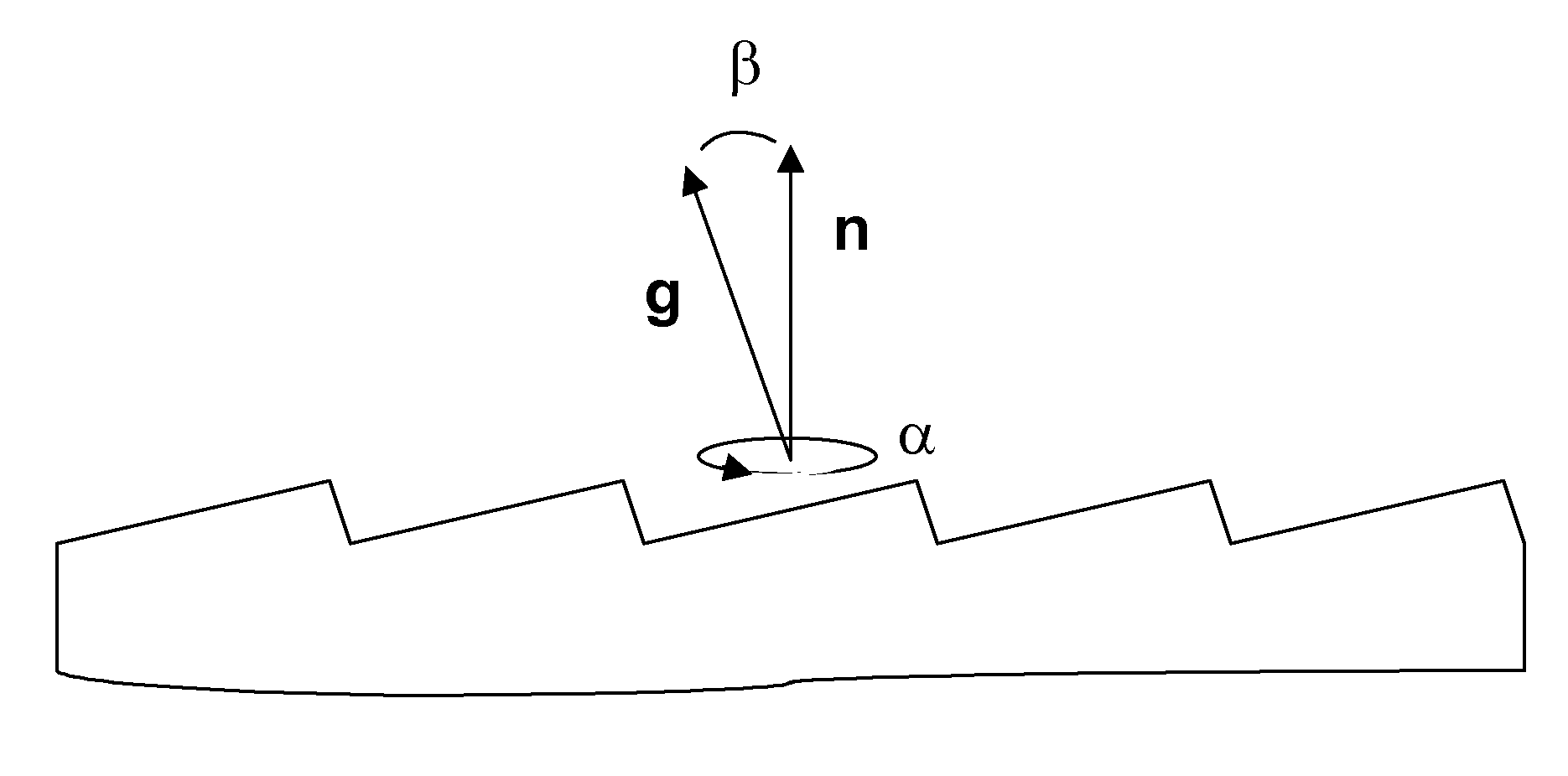
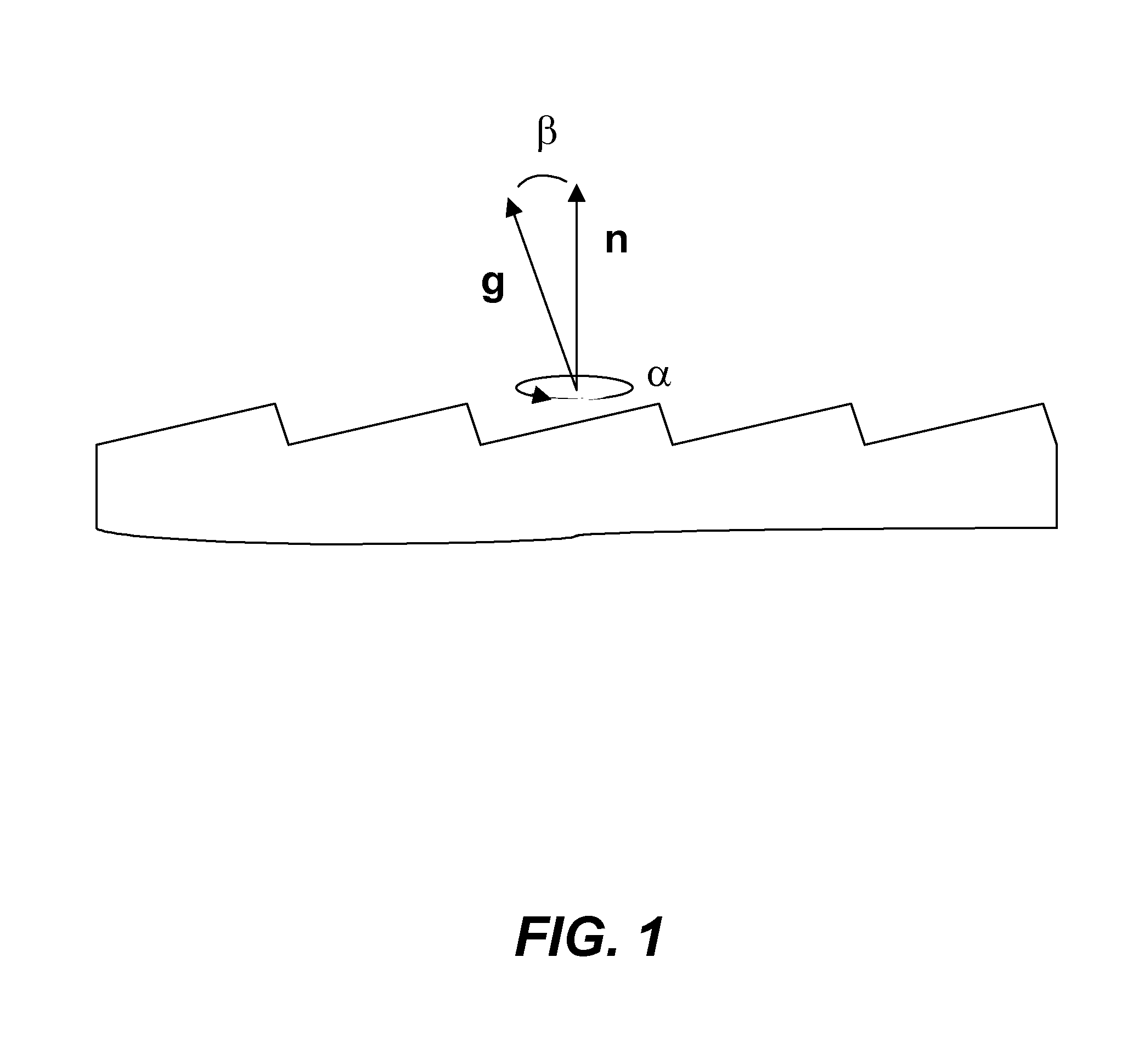
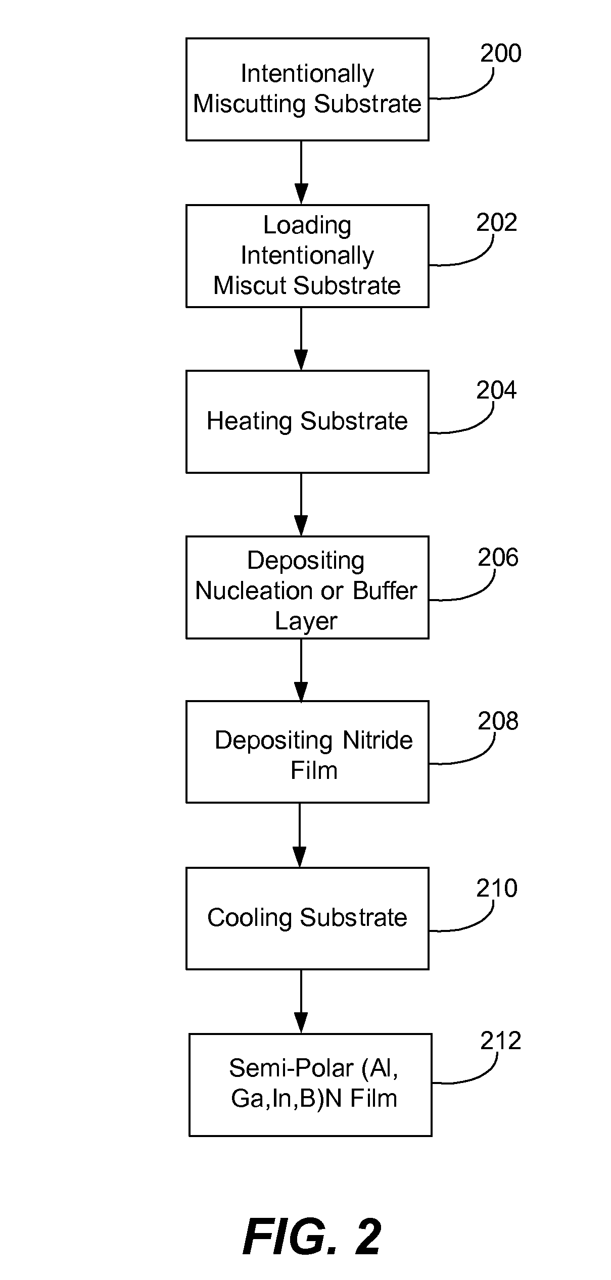
[0055]The present invention describes a method for growing semipolar nitride semiconductor films via techniques comprising, but not limited to, MOCVD, HVPE or MBE, on {100} MgAl2O4 (spinel) substrates miscut in the direction and on {1-100} (m-plane) Al2O3 (sapphire) substrates miscut in the direction. The use of an intentionally miscut substrate provides step edges and / or kinks, as shown in FIG. 1, that serve as preferential nucleation sites for the growth of semipolar nitride layers. This, in turn, leads to improved layer properties, comprising, but not limited to, coalesce...


PUM

PropertyMeasurementUnit
sizeaaaaaaaaaa
sizeaaaaaaaaaa
temperatureaaaaaaaaaa

Abstract

A method for improved growth of a semipolar (Al,In,Ga,B)N semiconductor thin film using an intentionally miscut substrate. Specifically, the method comprises intentionally miscutting a substrate, loading a substrate into a reactor, heating the substrate under a flow of nitrogen and / or hydrogen and / or ammonia, depositing an InxGa1−xN nucleation layer on the heated substrate, depositing a semipolar nitride semiconductor thin film on the InxGa1−xN nucleation layer, and cooling the substrate under a nitrogen overpressure.

Description

CROSS-REFERENCE TO RELATED APPLICATIONS[0001]This application claims the benefit under 35 U.S.C. Section 119(e) of the following co-pending and commonly-assigned U.S. patent application:[0002]U.S. Provisional Patent Application Ser. No. 60 / 760,739, filed on Jan. 20, 2006, by John Kaeding, Michael Iza, Troy J. Baker, Hitoshi Sato, Benjamin A. Haskell, James S. Speck, Steven P. DenBaars and Shuji Nakamura entitled “METHOD FOR IMPROVED GROWTH OF SEMIPOLAR (Al,In,Ga,B)N;”[0003]which application is incorporated by reference herein.[0004]This application is related to the following co-pending and commonly-assigned application:[0005]U.S. patent application Ser. No. 11 / 372,914 filed Mar. 10, 2006, by Troy J. Baker, Benjamin A. Haskell, Paul T. Fini, Steven P. DenBaars, James S. Speck, and Shuji Nakamura, entitled “TECHNIQUE FOR THE GROWTH OF PLANAR SEMI-POLAR GALLIUM NITRIDE,” now U.S. Pat. No. 7,220,324, issued May 22, 2007, which application claims the benefit under 35 U.S.C. Section 119(...

Claims


Application Information

Patent Timeline
Patent Type & Authority Patents(United States)
IPC IPC(8): H01L21/00H01L29/00
CPCC30B23/025C30B25/02C30B25/18C30B25/183C30B29/403C30B29/406H01L21/0242H01L21/02433H01L21/0254H01L21/0262H01L21/02378H01L33/007H01L21/02458H01L21/02293H01L2924/1033
Inventor KAEDING, JOHN F.LEE, DONG-SEONIZA, MICHAELBAKER, TROY J.SATO, HITOSHIHASKELL, BENJAMIN A.SPECK, JAMES S.DENBAARS, STEVEN P.NAKAMURA, SHUJI
Owner JAPAN SCI & TECH CORP
Why Eureka
Try Eureka