Vertical organic transistor
a vertical organic transistor and transistor technology, applied in transistors, solid-state devices, thermoelectric devices, etc., can solve the problems of difficult to obtain a sub-micron channel length in an organic semiconductor, difficult to reduce etc., to achieve effective control of the characteristics of the transistor, the effect of reducing the distance between the source and the drain
- Summary
- Abstract
- Description
- Claims
- Application Information
AI Technical Summary
Benefits of technology
Problems solved by technology
Method used
Image

Examples
embodiment i
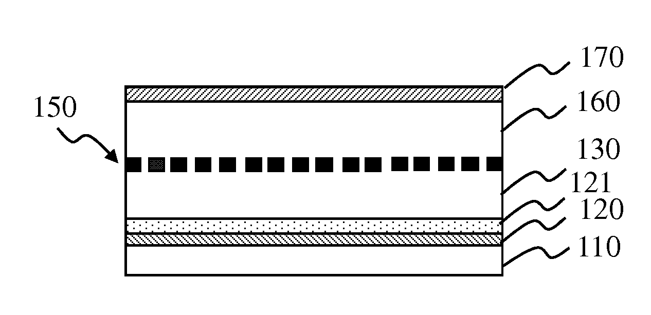
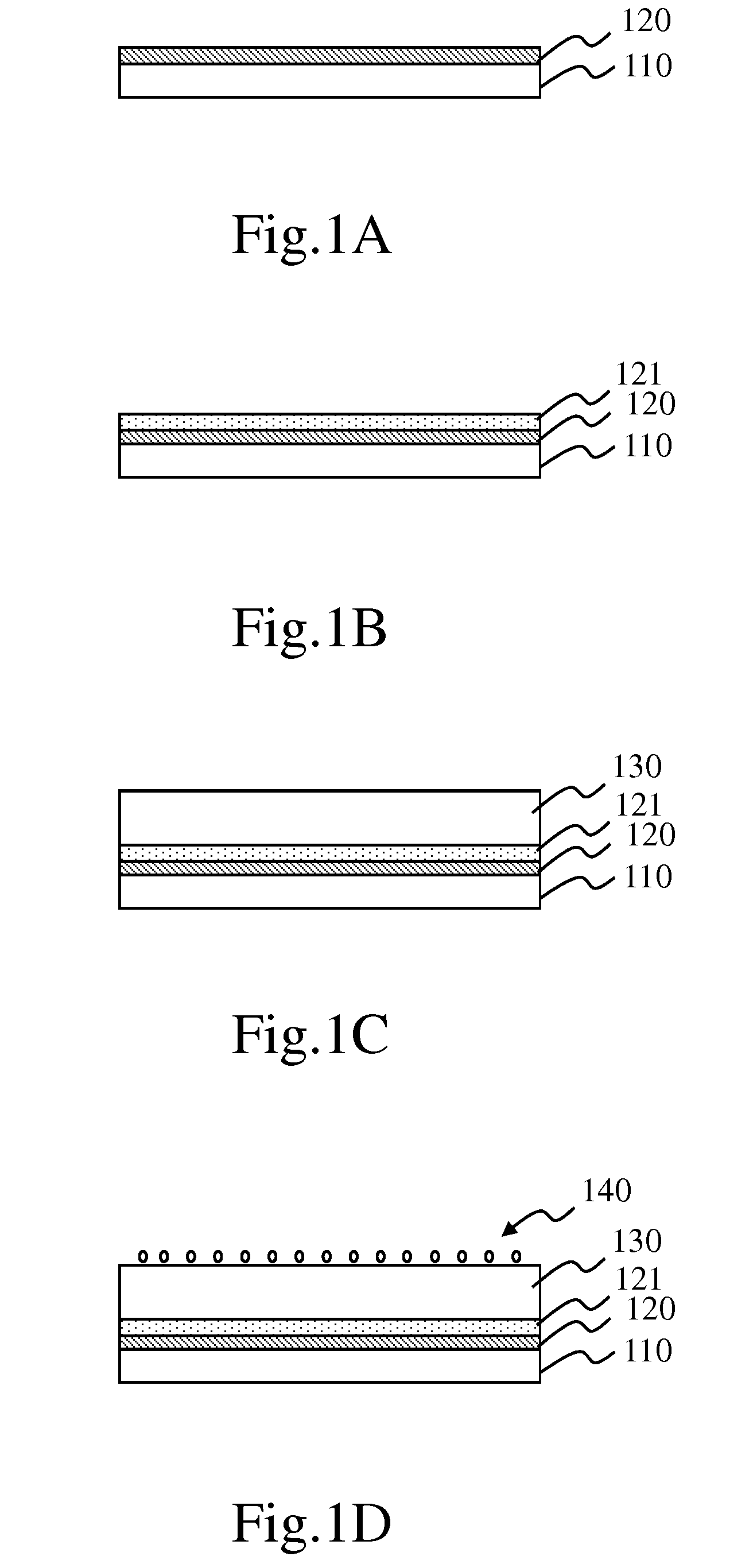
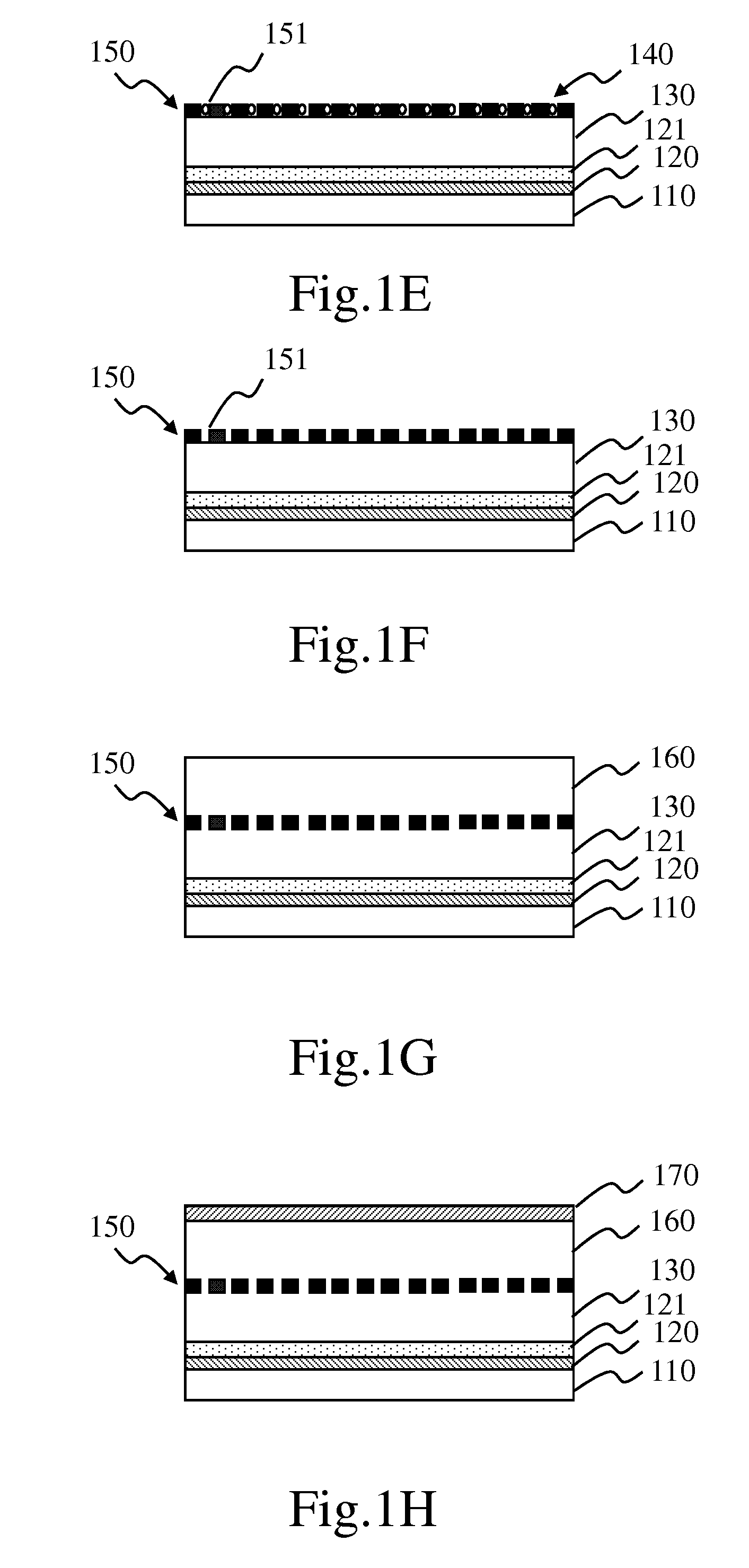
[0038]Refer to from FIG. 1A to FIG. 1H diagrams schematically showing the process of fabricating the vertical organic transistor according to Embodiment I of the present invention.
[0039]Refer to FIG. 1A. Firstly, a glass substrate 110 having an ITO (Indium-Tin-Oxide) conductive layer 120 is provided. Alternatively, the substrate 110 may also be a flexible substrate.
[0040]Refer to FIG. 1B. Next, the ITO conductive layer 120 is etched to define an emitter region; then, acetone, isopropyl alcohol and oxygen plasma are sequentially used to clean the ITO glass substrate 110; PEDOT:PSS (Poly(3,4-ethylenedioxythiophene) poly(styrenesulfonate)) is spin-coated on the ITO glass substrate 110 and then annealed in vacuum at a temperature of 200° C. for 10 minutes to obtain a conducting polymer 121 having a thickness of about 50 nm.
[0041]Refer to FIG. 1C. Next, a P3HT (poly-(3-hexylthiophene)) solution is spin-coated on the conducting polymer 121 and then annealed in vacuum at a temperature of 1...
embodiment ii
[0064]Refer to from FIG. 16A to FIG. 16D diagrams schematically showing the process of fabricating the vertical organic transistor according to Embodiment II of the present invention.
[0065]Refer to FIG. 16A. A copolymer is spin-coated on the emitter 220 to form an insulating layer 230. Refer to FIG. 16B. Next, the insulating layer 230 is fabricated into a perforate structure 240. Refer to FIG. 16C. Next, a metal is deposited on the perforate structure 240 to form a grid 250 with openings. Refer to FIG. 16D. Next, an organic semiconductor material is spin-coated on the grid 250 to form an organic semiconductor layer 260, and then a metal is deposited on the organic semiconductor layer 260 to form a collector 270. Thus, a vertical organic transistor is completed.
[0066]In this embodiment, the insulating layer 230 may be an aluminum oxide layer, wherein aluminum is vapor-deposited on the emitter 220, and the aluminum layer is processed with an appropriate method, such as an anodic treat...
embodiment iii
[0067]Refer to from FIG. 17A to FIG. 17F diagrams schematically showing the process of fabricating the vertical organic transistor according to Embodiment III of the present invention.
[0068]Refer to FIG. 17A. A material on another substrate or the another substrate itself is appropriately processed to form a perforate structure 340. Refer to FIG. 17B. Next, a sacrificial layer 380 is formed on the perforate structure 340. Refer to FIG. 17C. Next, a metal is deposited on the sacrificial layer 380 to form a grid 350. Refer to FIG. 17D. Next, the grid-deposited structure is flipped to overlay the substrate 310 having an emitter 320 and a first organic semiconductor layer 330. Refer to FIG. 17E. Next, the grid 350 is stuck to the first organic semiconductor layer 330. Refer to FIG. 17F. Next, an organic semiconductor material is spin-coated on the grid 350 to form a second organic semiconductor layer 360. Then, a metal is vapor-deposited on the second organic semiconductor layer 360 to ...
PUM
 Abstract
Description
Claims
Application Information
 - R&D Engineer
- R&D Manager
- IP Professional
- Industry Leading Data Capabilities
- Powerful AI technology
- Patent DNA Extraction
Browse by: Latest US Patents, China's latest patents, Technical Efficacy Thesaurus, Application Domain, Technology Topic.
© 2024 PatSnap. All rights reserved.Legal|Privacy policy|Modern Slavery Act Transparency Statement|Sitemap