Method for manufacturing semiconductor device

a semiconductor and manufacturing technology, applied in the field of semiconductor devices manufacturing, can solve the problems of low mass productivity, complex oscillator of solid lasers, and restriction of the output power of increasing harmonics, and achieve the effects of less electric power, simple structure, and resistance to vibration

Inactive Publication Date: 2010-04-20
SEMICON ENERGY LAB CO LTD
View PDF20 Cites 17 Cited by
  • Summary
  • Abstract
  • Description
  • Claims
  • Application Information

AI Technical Summary

Benefits of technology

[0012]In view of the aforementioned problems, it is an object of the present invention to manufacture a semiconductor device superior in electrical characteristics at low cost and with high throughput.
[0025]According to the present invention, a semiconductor film is heated by using a fiber laser. In comparison with an excimer laser or a conventional rod-type solid laser, a fiber laser has an oscillator with a simple structure and is resistant to vibration. Further, a fiber laser does not require an optical system for shaping a laser beam or requires only a simple optical system. Furthermore, a fiber laser consumers less electric power, and does not require maintenance and cooling water.
[0026]By using fiber lasers in combination, a beam having an arbitrary shape can be formed. According to the present invention by which a semiconductor device can be manufactured using a semiconductor film heated (crystallized) by irradiation with a fiber laser beam having such features, improvement of productivity and cost reduction for the semiconductor device can be achieved in comparison with the case of using an excimer laser or a conventional rod-type solid laser.

Problems solved by technology

However, since a solid laser has difficulty in forming a long linear beam, mass productivity is low.
This is a problem caused in the case of using a solid laser in a process for heating a semiconductor film.
However, this non-linear optical element has a threshold at which the element is damaged by input power of a fundamental wave; therefore, increasing output power of a harmonic has restriction.
Moreover, a solid laser has a complex oscillator which is sensitive to vibration, and further has problems of high power consumption, necessity of an optical system for beam shaping, necessity of maintenance and cooling water, and the like.

Method used


Image

  • Method for manufacturing semiconductor device
  • Method for manufacturing semiconductor device
  • Method for manufacturing semiconductor device

Examples


embodiment mode 1

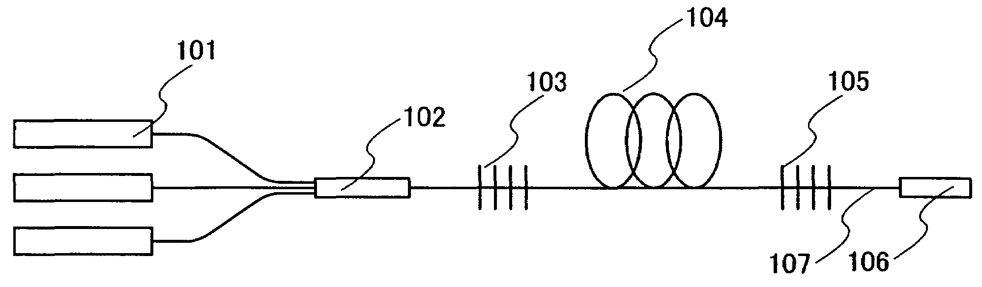
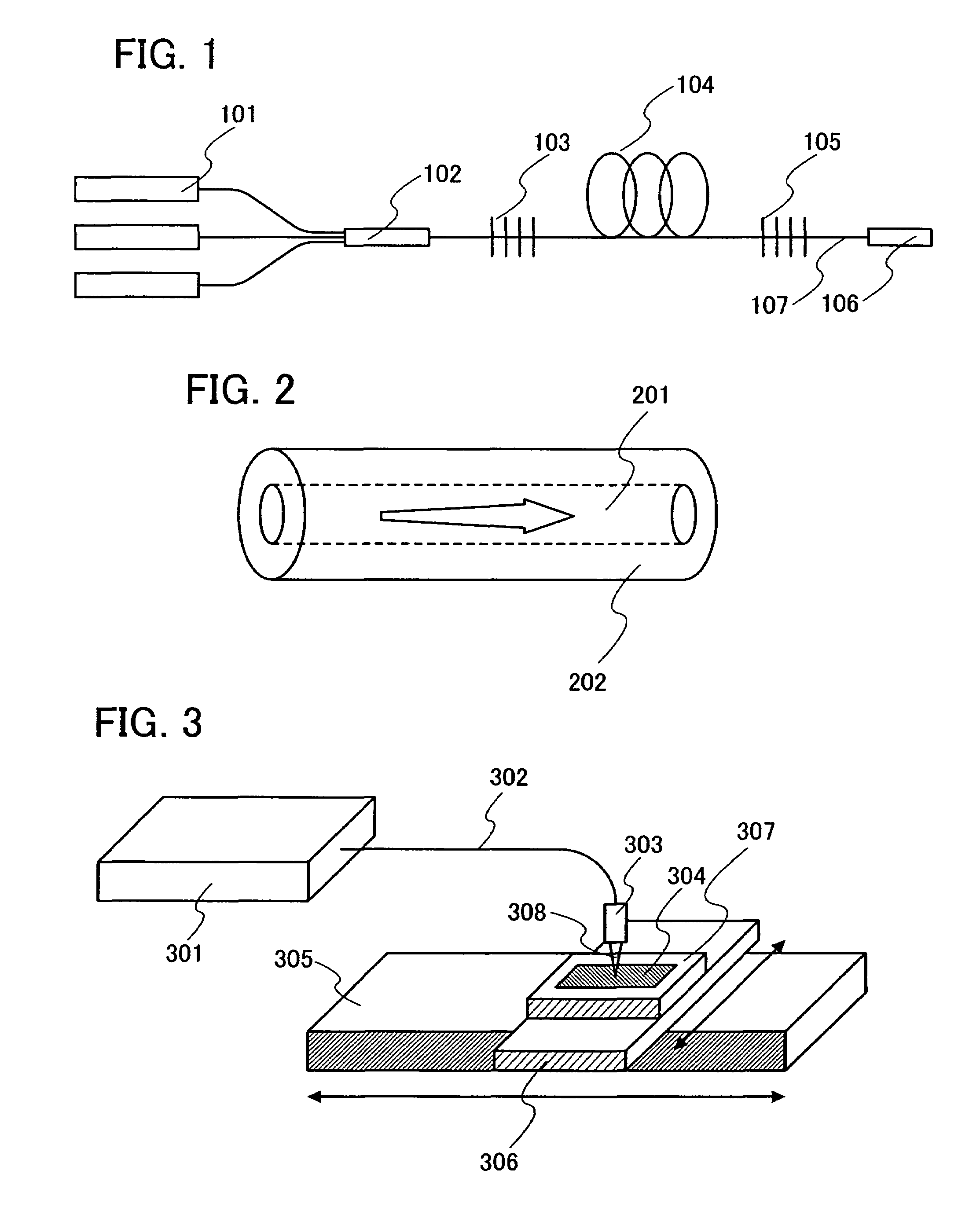
[0051]This embodiment mode will describe a structure of a method for manufacturing a semiconductor film with reference to drawings. In particular, a fiber laser used in the present invention will be described in detail.

[0052]A fiber laser uses an optical waveguide (optical fiber) as an oscillator. A structure of an oscillator of a fiber laser is described with reference to FIG. 1. A fiber laser has a laser diode (LD) 101 for excitation, an excited light combiner 102, fiber bragg gratings 103 and 105, an optical fiber 104 with its core doped with a laser medium (hereafter the optical fiber 104 is called an “active gain fiber”), and an output port 106. These appliances are connected to each other through a fiber cable 107. It is to be noted that the fiber laser can oscillate either in a continuous wave manner or a pulsed manner.

[0053]The excited light combiner 102 combines excited light emitted from a plurality of the laser diodes 101, and this combined light is inputted to the fiber ...

embodiment mode 2

[0063]This embodiment mode will describe a structure of a method for manufacturing a semiconductor film, with reference to drawings.

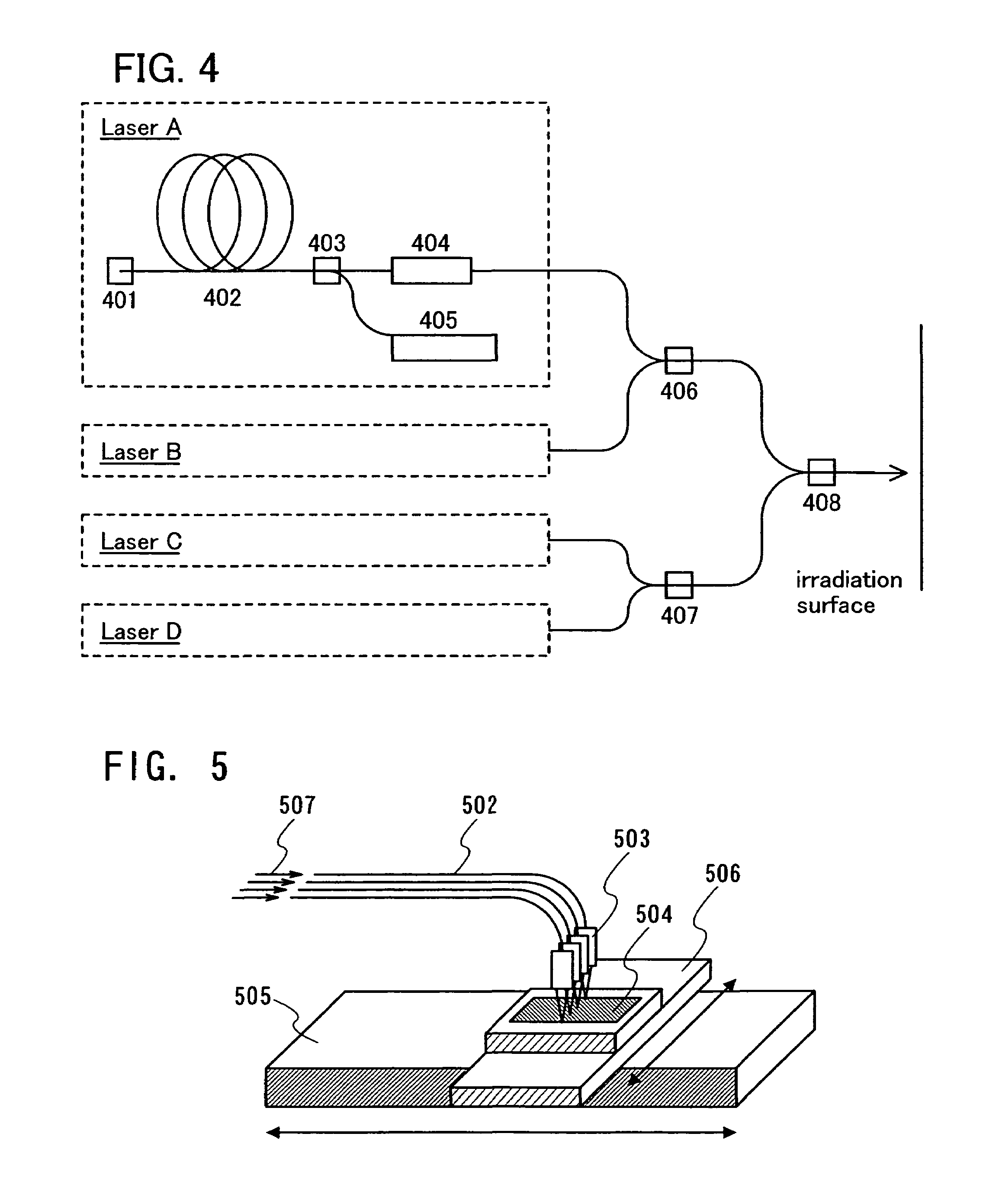
[0064]In this embodiment mode, laser beams emitted from a plurality of fiber laser oscillators are coupled by a coupler 406 and the coupled laser beam is applied to a manufacturing process of a semiconductor device (FIG. 4). For example, the laser irradiation is applied to a process of crystallization or activation of a semiconductor film.

[0065]In FIG. 4, a laser oscillator A includes a fiber bragg grating 401, an optical fiber 402 for amplifying light, a wavelength division multiplexer (WDM) 403, a non-linear optical element 404, and a laser diode 405. In this embodiment mode, a laser oscillator B, a laser oscillator C, and a laser oscillator D have the same structure as the laser oscillator A; however, the laser oscillators B, C, and D may have different structures from the laser oscillator A.

[0066]Laser beams emitted from the laser oscillators A and ...

embodiment mode 3

[0070]This embodiment mode will describe a different structure from that described in Embodiment Mode 2.

[0071]In this embodiment mode, a laser beam emitted from one fiber laser is divided into a plurality of laser beams by a coupler and the divided laser beams are delivered to a semiconductor film (irradiation surface).

[0072]For example, as shown in FIG. 21, a laser beam emitted from a laser oscillator A is divided by a coupler 411 and the divided laser beams are further divided by couplers 412 and 413. By irradiating a semiconductor film with the laser beams thus divided into four, the semiconductor film can be crystallized or activated.


PUM

PropertyMeasurementUnit
thicknessaaaaaaaaaa
diameteraaaaaaaaaa
diameteraaaaaaaaaa

Abstract

A semiconductor device having high electrical characteristics is manufactured at low cost and with high throughput. A semiconductor film is crystallized or activated by being irradiated with a laser beam emitted from one fiber laser. Alternatively, laser beams are emitted from a plurality of fiber lasers and coupled by a coupler to be one laser beam, and then a semiconductor film is irradiated with the coupled laser beam so as to be crystallized or activated.

Description

BACKGROUND OF THE INVENTION[0001]1. Field of Invention[0002]The present invention relates to a method for manufacturing a semiconductor device. The present invention particularly relates to a method for manufacturing a semiconductor device, in which a semiconductor film is heated by laser irradiation.[0003]2. Description of the Related Art[0004]In recent years, attention has been attracted to a technique for manufacturing thin film transistors (TFTs) by using a semiconductor thin film (with a thickness of about several nanometers to several hundred nanometers) formed over a substrate having an insulating surface. Thin film transistors are widely applied to electronic devices such as ICs and electro-optic devices, and development of thin film transistors as switching elements particularly for image display devices is urgently required.[0005]With the increase in size of image display devices and image sensors and in density of pixels (higher definition), elements using semiconductor t...

Claims


Application Information

Patent Timeline
Patent Type & Authority Patents(United States)
IPC IPC(8): H01L21/20
CPCB23K26/067B23K26/0738H01L27/1285H01L27/1266H01L21/2026H01L21/02683H01L21/02488H01L21/02422H01L21/02502H01L21/0242H01L21/02554H01L21/02425H01L21/02686H01L21/02678H01L21/02532H01L21/02381H01L21/02691H01L21/26H01L21/263H01L21/322H01L21/324H01L21/02675
Inventor SHIMOMURA, AKIHISA
Owner SEMICON ENERGY LAB CO LTD
Why Eureka
Try Eureka