Method and apparatus for imaging of scenes having large intensity variance

a technology of intensity variance and imaging method, applied in the field of electronic image generation and processing, can solve the problems of limited dynamic range of the electronic imaging apparatus, reduced detail in both shadowed and highlighted regions, and inability to capture most images, so as to reduce the sensitivity of the sub-array and reduce the intensity of the radiation falling

Inactive Publication Date: 2010-04-20
BARNEA DANIEL I +1
View PDF16 Cites 15 Cited by
  • Summary
  • Abstract
  • Description
  • Claims
  • Application Information

AI Technical Summary

Benefits of technology

[0017]ii. using the determined number of individual resets for each of the pixels, the residual value for each of the pixels, and a basic formula to determine the true image value for each of the pixels.The true image is comprised of an array of the true image values for each of the pixels. The combination of the reset mechanism for each pixel in conjunction with the use of the algorithm allows the determination of the true image without the necessity of providing electronic components for counting and remembering the number of times that each of the pixels was reset.
[0045]In another embodiment of the method of the invention the array of pixels is divided into a main group of pixels that are reset individually during the global exposure time interval whenever the voltage of the individual pixel of the main group reaches the reference voltage and a sparse sub-array of pixels whose integration time or sensitivity are altered such that the voltage of essentially all of the pixels of the sub-array reaches the reference voltage only if the light intensity on such pixel is higher then a predetermined maximal light intensity. The sub-array can be created by making a small hardware modification such that the pixels of the sub-array will have an integration time which is shorter than the global exposure time interval. A reduced sensitivity for the sub-array, could be achieved by use of an attenuating cover, which would reduce the intensity of the radiation falling of the covered pixels.
[0063]d. processing circuitry for carrying out at least part of an algorithm which uses the residual values of voltage to determine the true image value for each of the pixels.The true image acquired by the device is comprised of an array of the true image values for each of the pixels. The combination of the reset mechanism for each pixel in conjunction with the use of the algorithm allows the determination of the true image without the necessity of providing electronic components for counting and remembering the number of times that each of the pixels was reset.

Problems solved by technology

This is because electronic imaging apparatus exhibit limited dynamic range (response) i.e. the exposure time, which must be long enough for sufficient electronic detection of shadowed areas has to be at the same time, short enough to prevent saturation within high intensity areas.
This is an impossibility for most images.
The result of the limited dynamic range thus becomes a compromise, leading to reduced detail in both shadowed and highlighted regions.
Scenes with a high dynamic range, having both strong highlights and important shadow detail cannot be imaged with substantial fidelity.
The problems with these methods are in two areas.
Firstly, in each exposure, any movement in the image, real movement in the scene or camera movement, is translated differently in different exposure times and as a result the overall image, obtained by combining the different exposures, becomes distorted.
The second area in which problems arise is the response of the system to strong changes in the intensity of the scene.
In some systems the ratio of the exposures is kept constant, and then the coverage of the intensity variance of the real scene is not optimal.
In others, the exposures are changed independently and it takes long time to adapt to a new scene.
The common disadvantage of all the prior art methods of individual pixel reset, especially for CMOS cameras, is the additional cost of extra counting and memory circuitry, or analog type accumulators in other solutions, which must be added at each pixel site.
Also, there is the fact that additional circuit elements require space, thereby effectively reducing the light gathering ability of the array or increasing its size with attendant cost increases and signal / noise problems.
This solution, however, requires also cumbersome signal sampling and transfer procedures that affect the overall performance of the detector.
It may also impose limitations on the actual time each pixel can perform its reset cycle, if the design imposes the need for the “attention” of the central processing unit.
Therefore this method reduces the accuracy and sensitivity of the solution.

Method used


Image

  • Method and apparatus for imaging of scenes having large intensity variance
  • Method and apparatus for imaging of scenes having large intensity variance
  • Method and apparatus for imaging of scenes having large intensity variance

Examples


Embodiment Construction

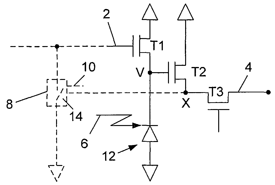
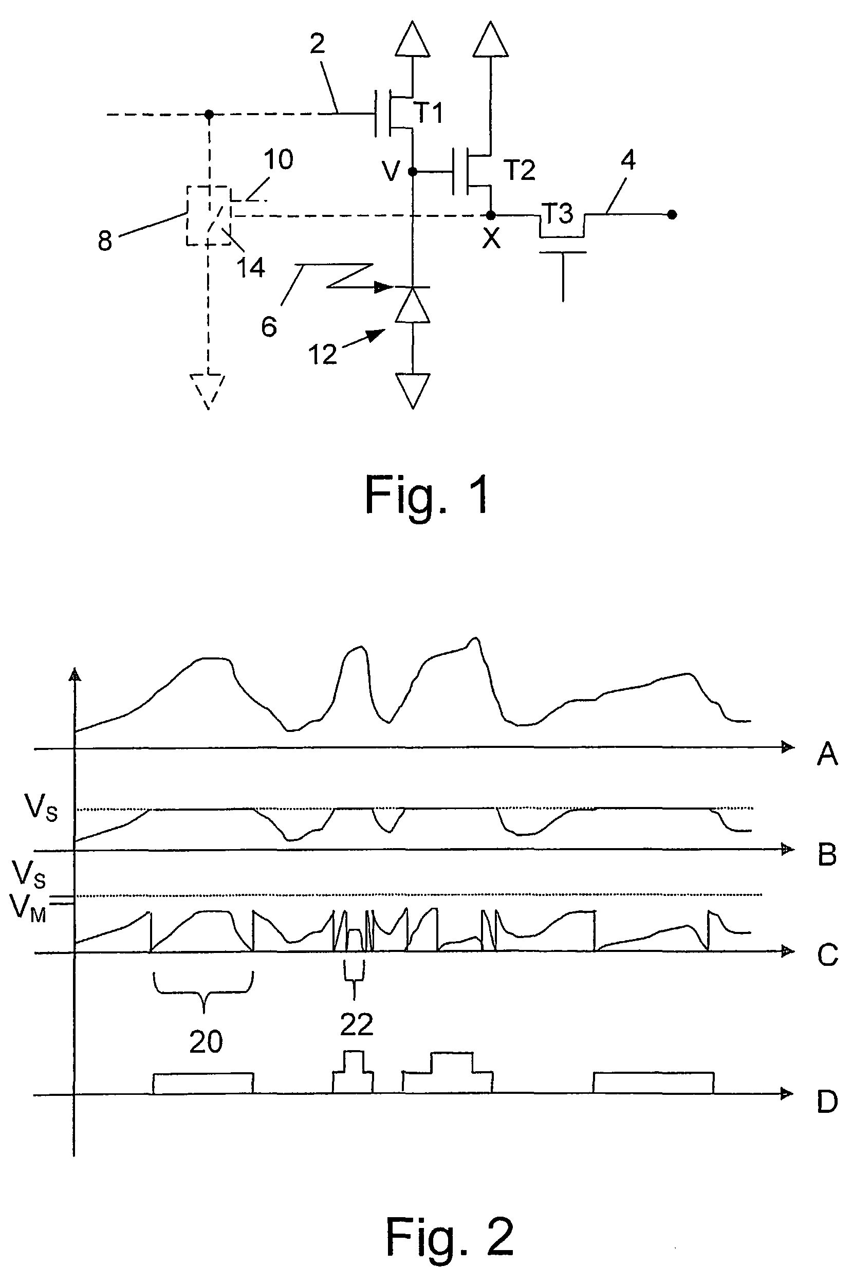
[0069]The present invention utilizes individual pixel reset to vary the residual integration time of individual pixels and processing of the signals from each pixel to increase the dynamic range of each pixel independently. The inventors estimate that the modifications needed to the area of a conventional chip will result in an increase in the chip area, and thus in production cost, of a maximum of some 15%. The relatively simple and low cost modification of the sensor chips will be introducible to the majority of cameras that are in use. This will render a dynamic range that will compete with cameras that derive an expanded dynamic range, by using more expensive technologies such as built in refrigeration methods, The method of the invention is applicable for different electronic image sensing devices and systems and is especially suitable for CMOS sensor chips. The basic dynamic range of a CMOS sensor is 8 bits or less, which is inferior to that of CCD chips. The method of the inv...


PUM


Abstract

The present invention is an electronic imaging device and method of expanding its dynamic range. The invention comprises modifying the imaging device by providing a comparator and reset trigger circuit located at or near the site of each of the pixels. The comparator triggers a reset mechanism when the voltage in the charged pixel reaches a reference voltage. During the global exposure time each individual pixel can be self-reset several times, depending on the intensity of the radiation incident upon it. At the end of the global exposure time, each pixel contains only the “residual value” of voltage that remains from the last individual self-reset to the end of the global integration time. An algorithm is implemented, which estimates and determines the number of resets undergone by each pixel during the global exposure time. From this number of resets the algorithm is able to reconstruct the true image. As opposed to prior art methods that make use of pixel reset the device of the invention does not contain electronic components for counting and remembering the number of times that each of the pixels was reset.

Description

FIELD OF THE INVENTION[0001]The present invention relates to the field of generating and processing of electronic images. In particular the invention relates to methods and apparatus for the capture and reproduction of improved intensity variance of such images.BACKGROUND OF THE INVENTION[0002]Numerous everyday scenes have a far greater intensity variance range than can be recorded on an electronic imaging apparatus (e.g., a still or video camera). This is because electronic imaging apparatus exhibit limited dynamic range (response) i.e. the exposure time, which must be long enough for sufficient electronic detection of shadowed areas has to be at the same time, short enough to prevent saturation within high intensity areas. This is an impossibility for most images. The result of the limited dynamic range thus becomes a compromise, leading to reduced detail in both shadowed and highlighted regions. The deep shadows are recorded as undifferentiated black and the bright highlights are...

Claims


Application Information

Patent Timeline
Patent Type & Authority Patents(United States)
IPC IPC(8): H04N3/15H04N5/243
CPCH04N5/23248H04N5/37455H04N5/35536H04N23/68H04N25/58H04N25/772H04N25/57
Inventor BARNEA, DANIEL I.SOREK, NOAM
Owner BARNEA DANIEL I
Why Eureka
Try Eureka