Transistor and routing layout for a radio frequency integrated CMOS power amplifier device

a technology of transistor, which is applied in the direction of amplifier combinations, amplifiers with min 3 electrodes or 2 pn junctions, semiconductor/solid-state device details, etc., can solve the problems of adversely affecting the performance and gain of the more expensive implementation of off-chip gaas technology than the integrated cmos power amplifier technology, and the inability to achieve the effect of reducing the cost of implementing off-chip ga

Inactive Publication Date: 2010-04-27
APPLE INC
View PDF2 Cites 6 Cited by
  • Summary
  • Abstract
  • Description
  • Claims
  • Application Information

AI Technical Summary

Problems solved by technology

Integration of radio frequency (RF) power amplifiers into complementary metal-oxide-semiconductor (CMOS) transceivers is one of the most challenging tasks in modern wireless communication products.
However, integration of the power amplifier is driven by the ever shrinking design footprint of state of the art hand-held wireless products.
Furthermore, implementing off-chip GaAs technology is more expensive than integrated CMOS power amplifier technology.
Consequently, increasing the path to the middle point virtual ground between the two sets of main core transistors increases the effective differential parasitic inductance to virtual ground which, in turn, adversely affects the performance and the gain of the integrated CMOS power amplifier 104.
This increased common-mode ground inductance also adversely affects the performance of the integrated CMOS power amplifier 104.

Method used


Image

  • Transistor and routing layout for a radio frequency integrated CMOS power amplifier device
  • Transistor and routing layout for a radio frequency integrated CMOS power amplifier device
  • Transistor and routing layout for a radio frequency integrated CMOS power amplifier device

Examples


Embodiment Construction

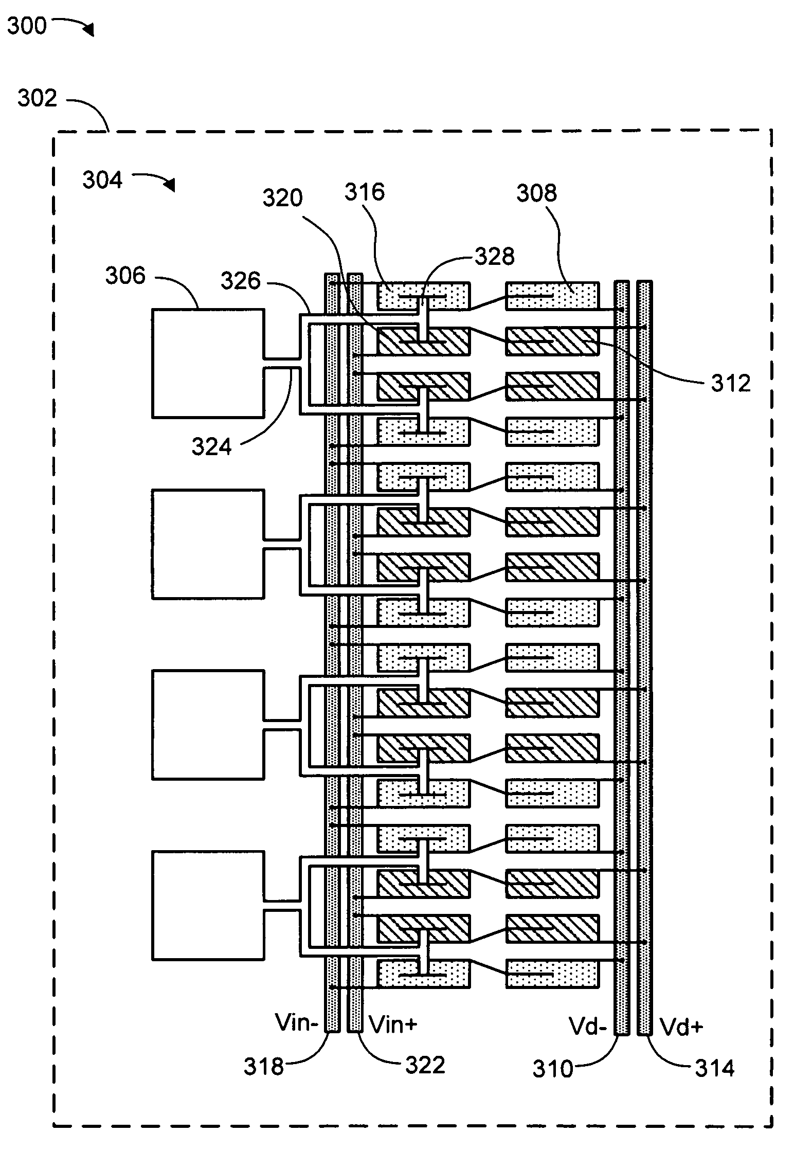
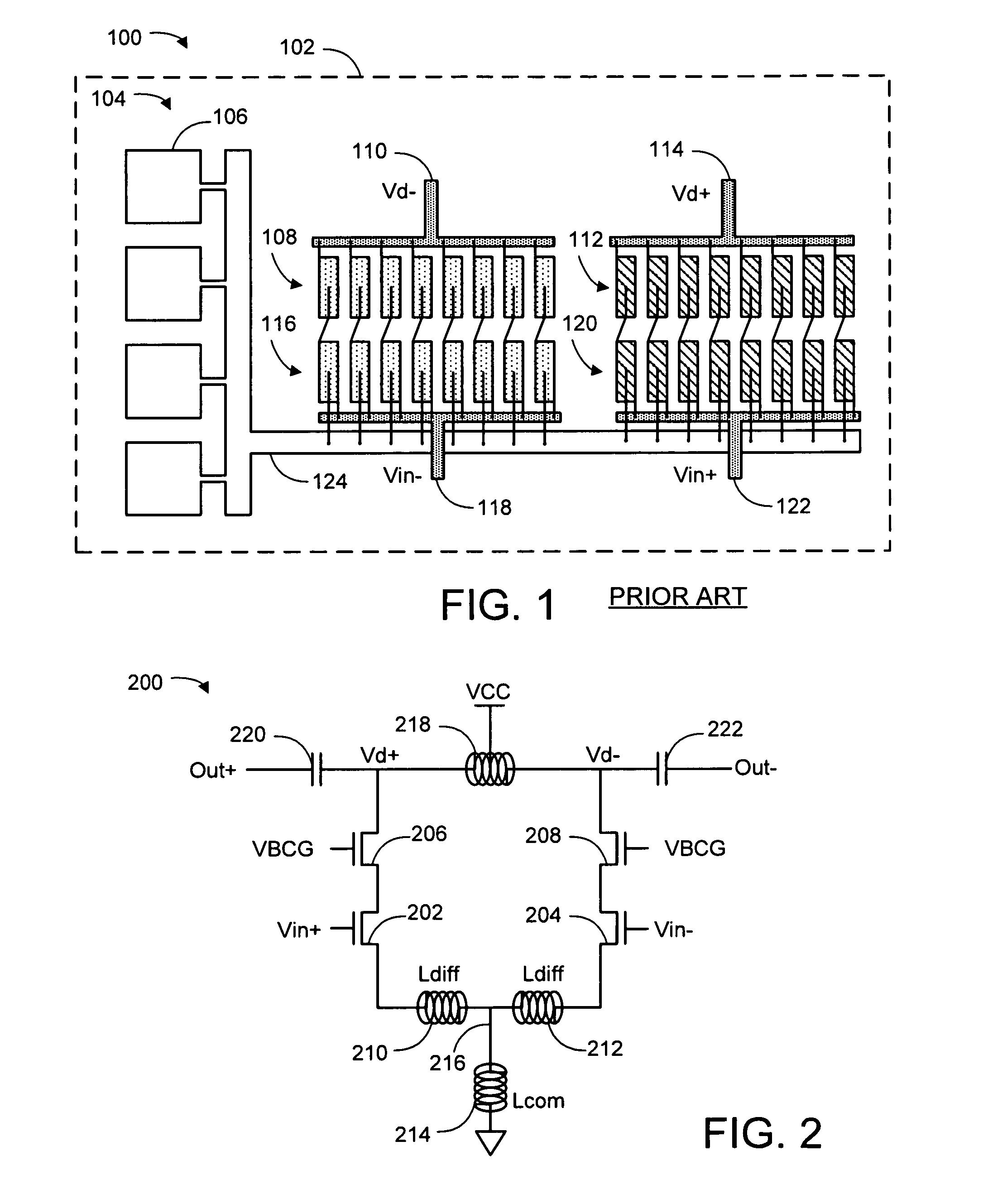
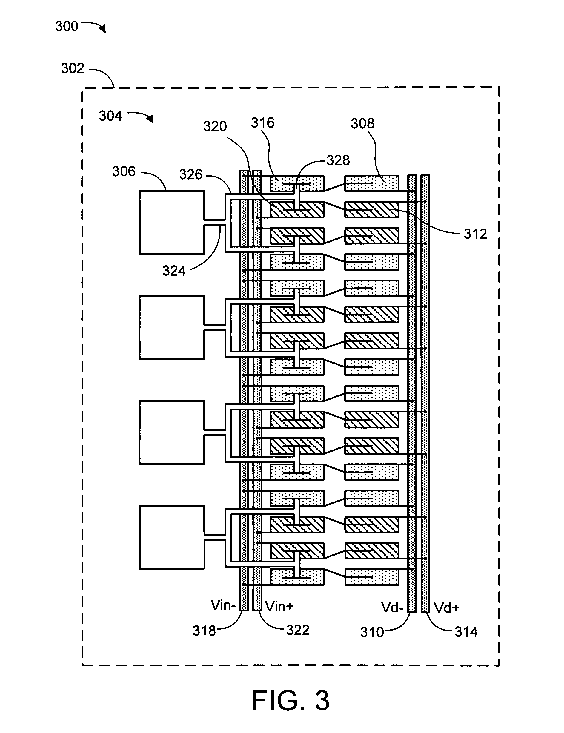
[0014]FIG. 2 depicts a schematic circuit diagram of one embodiment of a simplified representation of a radio frequency integrated CMOS power amplifier 200. Although certain component parts are shown in conjunction with the radio frequency differential power amplifier 200 of FIG. 2, other embodiments may include fewer or more component parts, or equivalent parts, to perform fewer or more power amplifier functions. Additionally, while the components of the radio frequency differential power amplifier 200 are shown in FIG. 2 as being separate components, these components may be integrated on a single integrated chip. Additionally, some of the components shown may be representative of inherent circuit characteristics rather than discrete devices.

[0015]The radio frequency differential power amplifier 200 includes a p-block common-source transistor 202, an n-block common-source transistor 204, a p-block common-gate transistor 206, and an n-block common-gate transistor 208. The p-block com...


PUM


Abstract

An integrated CMOS power amplifier system to improve amplifier performance, the integrated CMOS power amplifier system including a plurality of differential main amplifier cores, a plurality of ground pads, and a plurality of routes to connect the plurality of differential main amplifier cores to the plurality of ground pads. Each differential main amplifier core includes a pair of collocated main amplifier core transistors. Each ground pad is connected to a subset of the differential main amplifier cores. Embodiments of the integrated CMOS power amplifier system decrease parasitic inductance to ground and increase the transconductance and amplification of the integrated CMOS power amplifier system, thus improving performance.

Description

BACKGROUND OF THE INVENTION[0001]Integration of radio frequency (RF) power amplifiers into complementary metal-oxide-semiconductor (CMOS) transceivers is one of the most challenging tasks in modern wireless communication products. Deep sub-micron CMOS technologies allow the integration of such power amplifiers on single-chip transceivers. An RF power amplifier is a circuit that amplifies an input RF signal while delivering significant amount of RF output power to a load. Today most wireless products employ an off-chip power amplifier, typically gallium-arsenide (GaAs) based, to provide the required power levels. However, integration of the power amplifier is driven by the ever shrinking design footprint of state of the art hand-held wireless products. Furthermore, implementing off-chip GaAs technology is more expensive than integrated CMOS power amplifier technology. Unlike the single-ended GaAs PAs, CMOS power amplifiers are typically differential amplifiers. Differential configura...

Claims


Application Information

Patent Timeline
Patent Type & Authority Patents(United States)
IPC IPC(8): H03F3/14
CPCH01L23/66H03F3/195H03F3/245H03F3/45188H01L24/48H01L2924/30107H01L2223/6638H01L2223/6644H01L2223/6655H01L2924/3011H03F2203/45386H03F2203/45464H01L2224/48H01L2924/00H01L2924/14H01L2924/00014H01L2224/45099H01L2224/45015H01L2924/207
Inventor DEGANI, OFFIRRUBERTO, MARK
Owner APPLE INC
Why Eureka
Try Eureka