LED device having improved output and contrast

a technology of oled devices and outputs, applied in the direction of discharge tubes/lamp details, discharge tubes luminescnet screens, electric discharge lamps, etc., can solve the problems of poor efficiency, light emission, and low efficiency of these devices in comparison with typical oled devices, so as to improve light efficiency and ambient contrast

Active Publication Date: 2010-05-04
GLOBAL OLED TECH
View PDF27 Cites 20 Cited by
  • Summary
  • Abstract
  • Description
  • Claims
  • Application Information

AI Technical Summary

Problems solved by technology

Recombination of holes and electrons occurs within the light emitting layer and results in emission of light.
Because of problems such as aggregation of the quantum dots in the emitter layer, the efficiency of these devices was rather low in comparison with typical OLED devices.
The efficiency was even poorer when a neat film of quantum dots was used as the emitter layer (Hikmet et al., Journal of Applied Physics 93, 3509 (2003)).
The poor efficiency was attributed to the insulating nature of the quantum-dot layer.
Regardless of improvements in efficiency, these hybrid devices still suffer from all of the drawbacks associated with pure OLED devices.
The resulting device had a poor external quantum efficiency of 0.001 to 0.01%.
These organic ligands are insulators and would result in poor electron and hole injection into the quantum dots.
In addition, the remainder of the structure is costly to manufacture, due to the usage of electron and hole semiconducting layers grown by high-vacuum techniques, and the usage of sapphire substrates.
However, electroluminescent devices generally suffer from poor ambient contrast because of the reflectivity of the reflective electrode.
Such a reflector tends to reflect ambient light thus reducing the contrast between the emitted light and the ambient light and decreasing the image quality of the LED device.
However, such polarizers are expensive and also absorb as much as 40% of the emitted light.
Such louver films are typically employed on the top surface of a display device, and while effective at reducing viewing angles, typically have not been suggested for use in displays with improved light output and sharpness of display images.
It has also been found, that one of the key factors that limits the efficiency of LED devices is the inefficiency in extracting the photons generated by the electron-hole recombination out of the LED devices.
Due to the high optical indices of the materials used, most of the photons generated by the recombination process are actually trapped in the devices due to total internal reflection.
In general, up to 80% of the light may be lost in this manner.
In any of these LED structures, the problem of trapped emitted light and reflected ambient light remains.
Moreover, the contrast of the device is not improved under diffuse illumination.
Moreover, trapped light may propagate a considerable distance horizontally through the cover, substrate, or organic layers before being scattered out of the device, thereby reducing the sharpness of the device in pixellated applications such as displays.
The particular arrangements, however, may still result in reduced sharpness of the device and does not improve contrast.
Such disclosed designs, however, do not improve the contrast of the device.
While such methods are useful, the presence of a reflective electrode still decreases the ambient contrast significantly.
As noted above, circular polarizers may be employed, but applicants have determined that light-extraction techniques such as scattering layers tend to be incompatible with such polarizers.

Method used


Image

  • LED device having improved output and contrast
  • LED device having improved output and contrast
  • LED device having improved output and contrast

Examples


Embodiment Construction

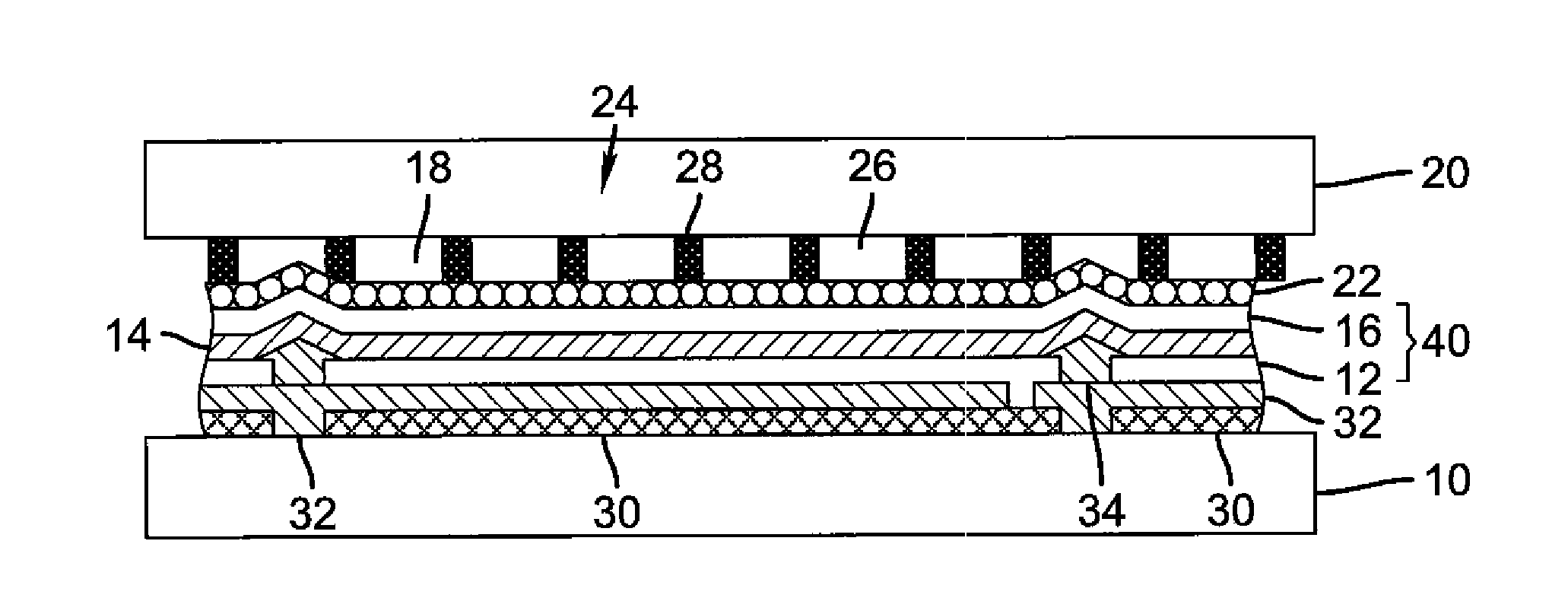
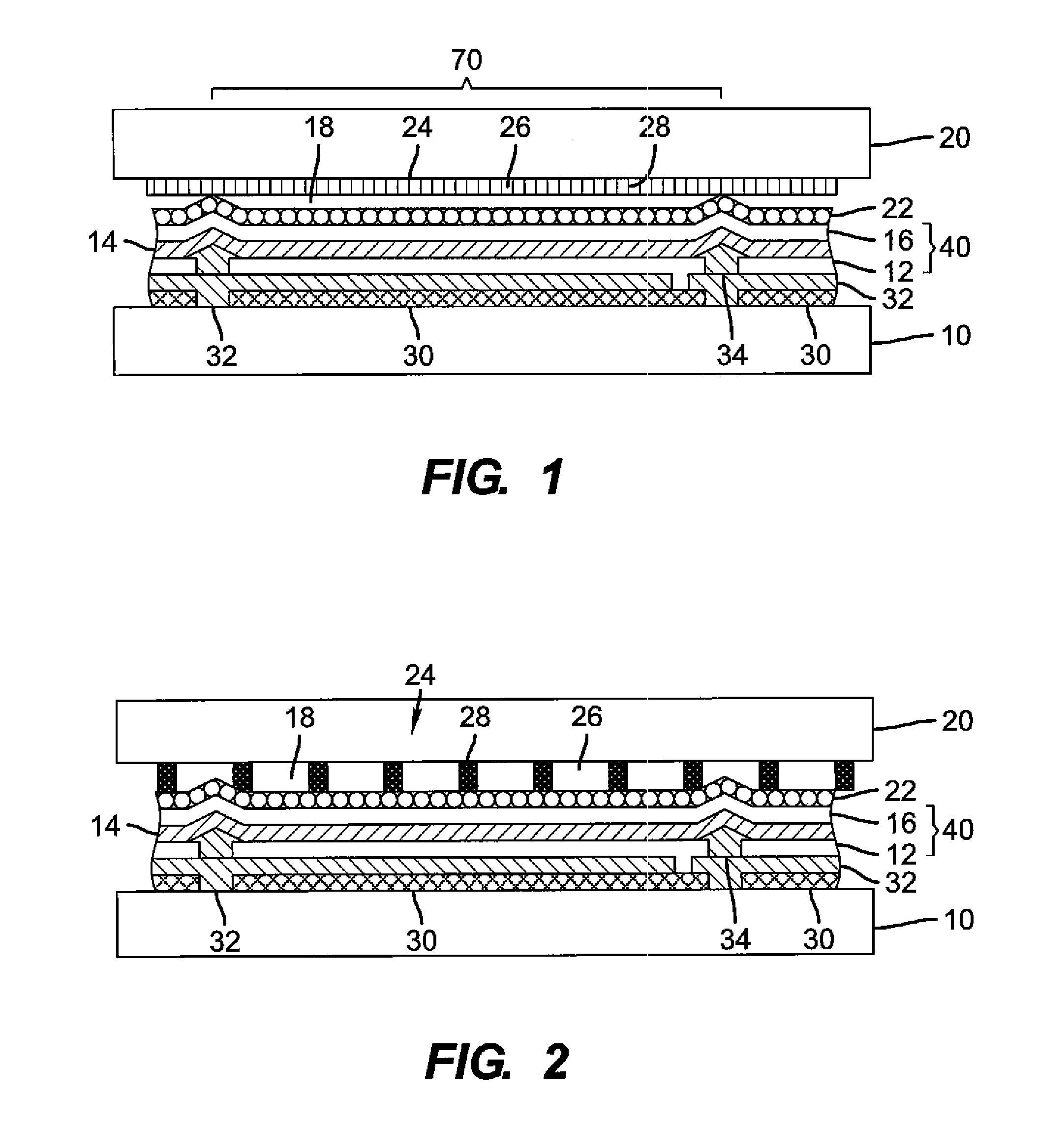
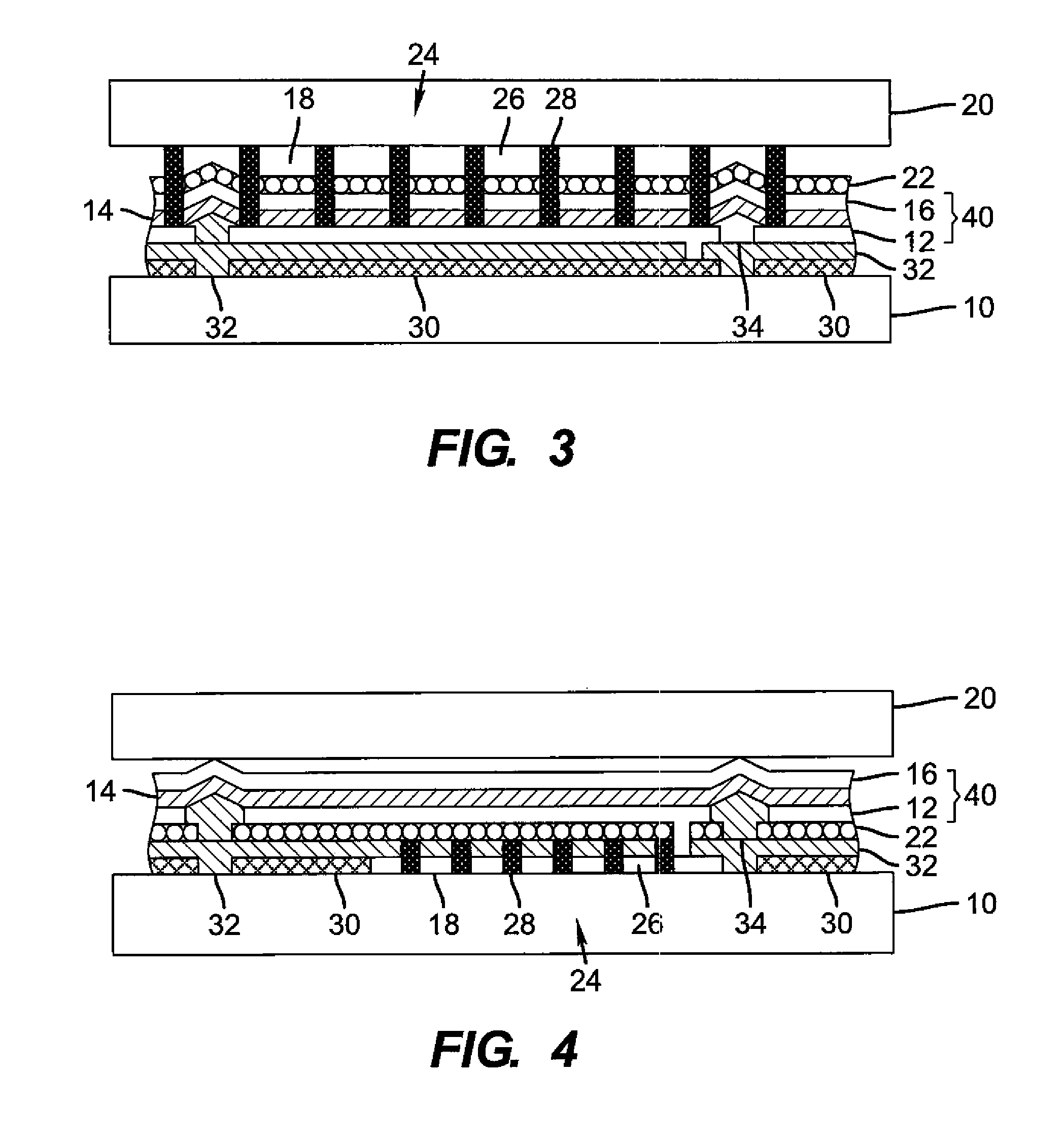
[0039]Referring to FIG. 1, in accordance with one embodiment of the present invention, an light-emitting diode (LED) device, comprises an LED 40 formed over a substrate 10 having a first patterned electrode 12 defining independently controllable light-emitting areas 70, and a transparent second electrode 16 formed over the first electrode, wherein one or more EL unit(s) 14 are formed between the electrodes 12 and 16, the EL unit(s) 14 having a first optical index. A transparent cover 20 is formed over the LED 40 and has a second optical index, and light is emitted through the transparent cover 20. A light-scattering layer 22 is formed between the cover 20 and substrate 10 for scattering light. A low-index element 18 having an optical index lower than the first and second optical indices is formed between the scattering layer 22 and the transparent cover 20. A contrast-enhancement layer 24 comprising a plurality of alternating light-absorbing portions 28 and light-transmissive portio...


PUM


Abstract

An electroluminescent (EL) device having an LED formed on a substrate with at least two electrodes formed over the substrate, and an EL unit formed between the electrodes. At least one of the electrodes is transparent. At least one of the electrodes is patterned to define independently controllable light-emitting areas. A cover is formed over the LED. The cover or substrate is transparent. A light-scattering layer is formed between the cover and substrate for scattering light. A low-index element, having an optical index lower than other optical indices, is formed between the scattering layer and the transparent cover or substrate. Additionally, a contrast-enhancement layer includes alternating light-absorbing portions and light-transmissive portions formed in the layer located between the light-scattering layer and the transparent substrate or cover through which light is emitted, wherein the light-absorbing portions and light-transmissive portions are located in each light-emitting area.

Description

CROSS-REFERENCE RELATED APPLICATIONS[0001]This is a continuation-in-part of application Ser. No. 11 / 297,196, filed on Dec. 8, 2005, now U.S. Pat. No. 7,466,075, entitled “OLED Device Having Improved Output and Contrast”, in the names of Ronald S. Cok and Lee W. Tutt.FIELD OF THE INVENTION[0002]The present invention relates to electroluminescent devices, and more particularly, to electroluminescent device structures for improving light output and contrast.BACKGROUND OF THE INVENTION[0003]Electroluminescent devices are a promising technology for flat-panel displays and area illumination lamps. These devices rely upon thin-film layers of materials coated upon a substrate, and include organic, inorganic and hybrid inorganic-organic light-emitting diodes. The thin-film layers of materials can include, for example, organic materials, quantum dots, fused inorganic nano-particles, electrodes, conductors, and silicon electronic components as are known and taught in the LED art.[0004]Irrespec...

Claims


Application Information

Patent Timeline
Patent Type & Authority Patents(United States)
IPC IPC(8): H01J1/62H01J63/04
CPCH01L51/5284H01L51/5268H05B33/22H01J1/70H01L33/00H01L33/44H01L2933/0091H01L33/58H01L33/46H10K50/854H10K50/865H01J1/62
Inventor COK, RONALD S.TUTT, LEE W.
Owner GLOBAL OLED TECH
Why Eureka
Try Eureka