Surface defect inspection method and apparatus

a technology of surface defect and inspection method, which is applied in the direction of optically investigating flaws/contamination, measurement devices, instruments, etc., can solve the problems of lowering detection sensitivity, achieve improved sn ratio, reduce sn ratio, and reduce detection sensitivity

Inactive Publication Date: 2010-05-04
HITACHI HIGH-TECH CORP
View PDF17 Cites 24 Cited by
  • Summary
  • Abstract
  • Description
  • Claims
  • Application Information

AI Technical Summary

Benefits of technology

[0005]A problem to be solved by the present invention will be described. The distribution of the scattered light caused by the defect with the size corresponding to 1 / 10 of the illumination wavelength becomes isotropic. So the SN ratio is improved by adding the multi-directionally detected signals, which makes it possible to detect the tiny defect. Meanwhile, the defect which causes the distribution of the scattered light to be anisotropic reduces the SN ratio by adding the multi-directionally detected signals, thus lowering the detection sensitivity. The surface defect inspection with respect to the semiconductor substrate is required to be performed with high sensitivity irrespective of the defect type.

Problems solved by technology

Meanwhile, the defect which causes the distribution of the scattered light to be anisotropic reduces the SN ratio by adding the multi-directionally detected signals, thus lowering the detection sensitivity.

Method used


Image

  • Surface defect inspection method and apparatus
  • Surface defect inspection method and apparatus
  • Surface defect inspection method and apparatus

Examples


Embodiment Construction

[0057]An embodiment of the present invention will be described.

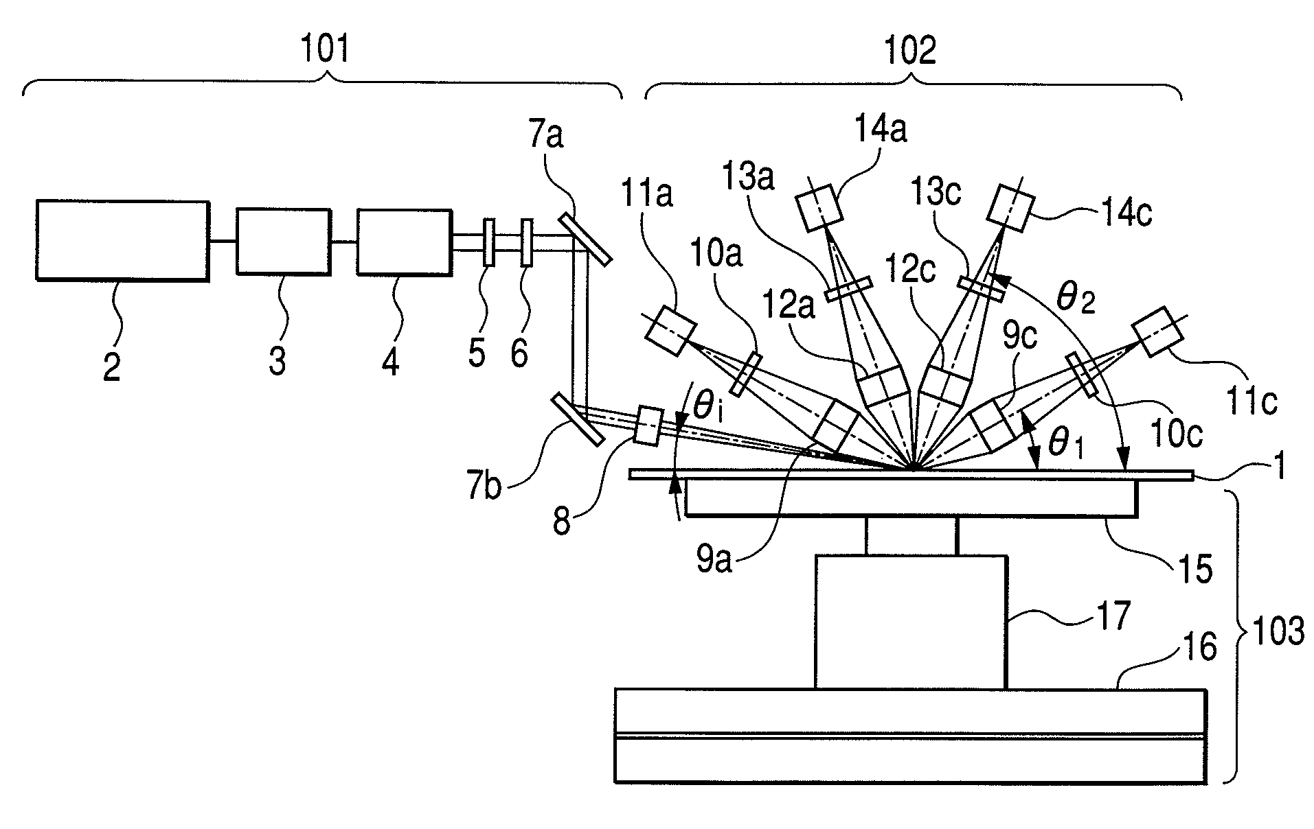
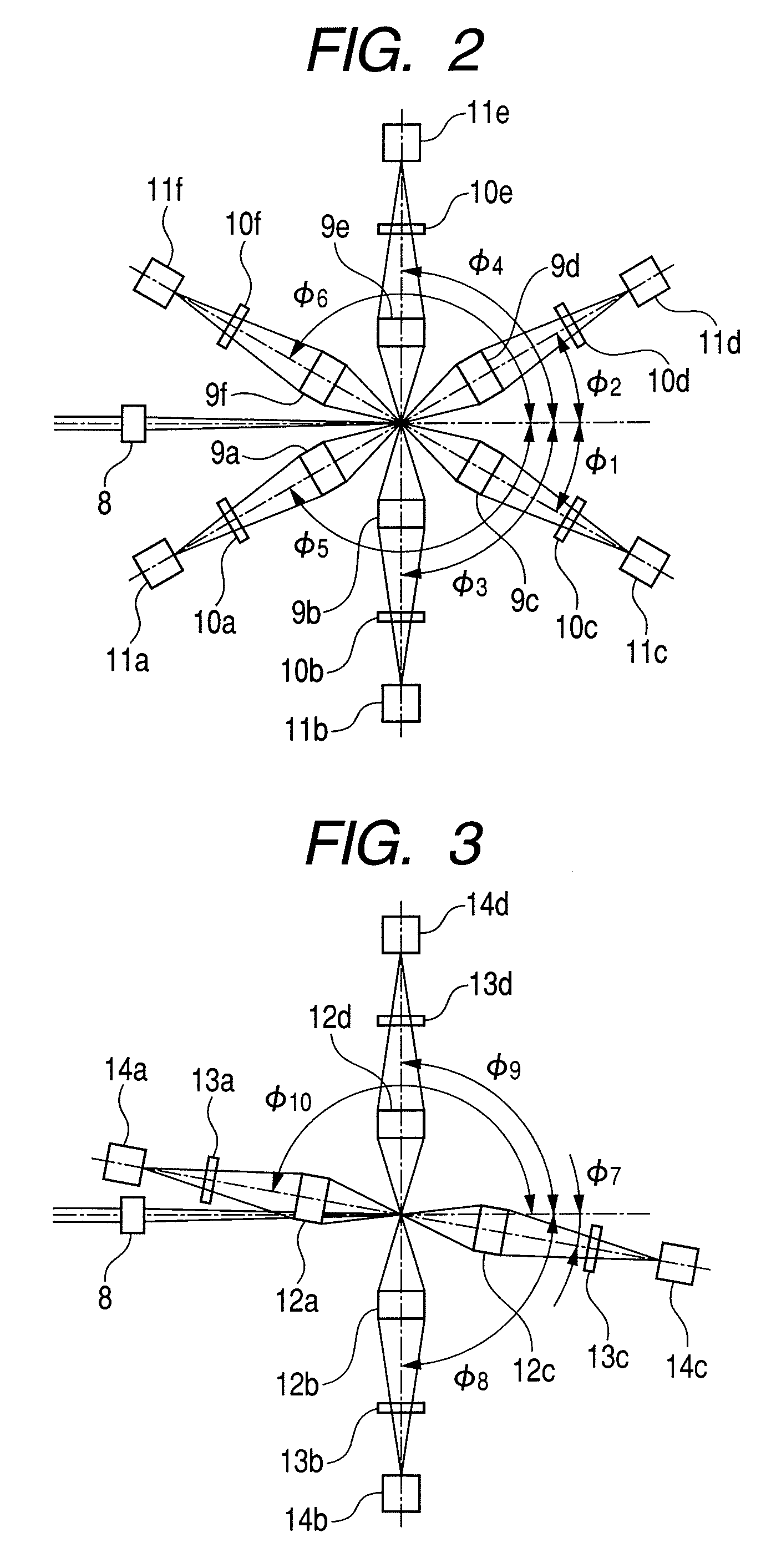
[0058]FIGS. 1 to 3 show an example of an apparatus for detecting the defect / foreign matter on the semiconductor wafer before forming the circuit pattern. FIG. 1 is a side view, FIG. 2 is a plan view of a low angle detection system, and FIG. 3 is a plan view of a high angle detection system. The apparatus shown in FIG. 1 includes an illumination optical system 101, a detection optical system 102 and a wafer stage 103. The illumination optical system 101 includes a laser light source 2, an attenuator 3, a beam expander 4, wavelength plates 5, 6, and a condensing lens 8.

[0059]The laser beam from the laser light source 2 has its light intensity adjusted to the required value by the attenuator 3. The beam radius of the laser is expanded by the beam expander 4, and the polarization direction of the illumination is set by the wavelength plates 5, 6. The condensing lens 8 performs condensing and illumination to the detection are...


PUM

PropertyMeasurementUnit
sizeaaaaaaaaaa
illumination elevation angle θiaaaaaaaaaa
elevation angleaaaaaaaaaa

Abstract

A surface defect inspection apparatus is structured to add detection signals of multi-directionally detected scattered lights to detect a tiny defect and to individually process the respective detection signals to prevent an error failing to detect an anisotropic defect.

Description

CLAIM OF PRIORITY[0001]The present application claims priority from Japanese Application JP 2007-115004 filed on Apr. 25, 2007, and Japanese Application JP 2007-156385 filed on Jun. 13, 2007, the content of which is hereby incorporated by references into this application.BACKGROUND OF THE INVENTIONField of the Invention[0002]The present invention relates to a surface defect inspection method and a surface defect inspection apparatus for detecting a tiny foreign matter / defect on the surface of the semiconductor substrate and the like with high sensitivity at high speeds.[0003]On the manufacturing line of the semiconductor substrate or the thin film substrate, the inspection with respect to the defect and foreign matter on the surface of the semiconductor substrate or the thin film substrate is performed for the purpose of maintaining and further improving the product yield. For example, the sample of the semiconductor substrate prior to formation of the circuit pattern requires detec...

Claims


Application Information

Patent Timeline
Patent Type & Authority Patents(United States)
IPC IPC(8): G01N21/00G01N21/88
CPCG01N21/9501G01N2021/4716
Inventor OSHIMA, YOSHIMASANAKAO, TOSHIYUKIMATSUI, SHIGERU
Owner HITACHI HIGH-TECH CORP
Why Eureka
Try Eureka