Integrated thin-film sensors and methods

a technology of integrated thin-film sensors and sensors, applied in the field ofluminescent chemical and biological sensors, can solve the problems of long response time, increased complexity, size and cost, and long response time of electronic sensors, and achieve the effect of compact field-deployable devices

Inactive Publication Date: 2010-05-18
IOWA STATE UNIV RES FOUND
View PDF2 Cites 16 Cited by
  • Summary
  • Abstract
  • Description
  • Claims
  • Application Information

AI Technical Summary

Benefits of technology

[0009]The invention provides structural integration of PL-based chemical and biological sensors, which results in very compact, field-deployable devices.

Problems solved by technology

However, electrochemical sensors consume analytes, have long response times, are limited with regard to in vivo use, and are susceptible to poisoning by various contaminants.
However, the need to incorporate optical components to convey light to the sensor and to collect the PL for readout increases complexity, size, and costs.
Thus, single crystal III-V compound inorganic LEDs do not permit simple fabrication of integrated multisensor arrays.
Light sources such as lasers or inorganic LEDs either may be difficult to integrate with the other components due to size, geometrical, or operational constraints, or they involve intricate integration procedures.
In addition, they often generate heat, which can damage the sensing element or analyte.
In spite of potential widespread applications, the PD and light sources necessary to excite their PL typically have not been fully integrated with the sensing element.
Consequently, the unintegrated devices are relatively bulky, costly, require trained operators, and are limited in their applications.
The need to incorporate additional components such as optical fibers and their couplers to guide the light back and forth increases the size, cost, and complexity of the unit.

Method used


Image

  • Integrated thin-film sensors and methods
  • Integrated thin-film sensors and methods
  • Integrated thin-film sensors and methods

Examples


example

Manufacture of a Preferred Structurally Integrated Sensor

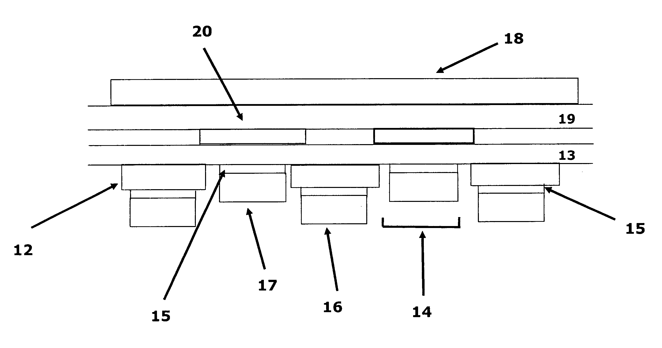
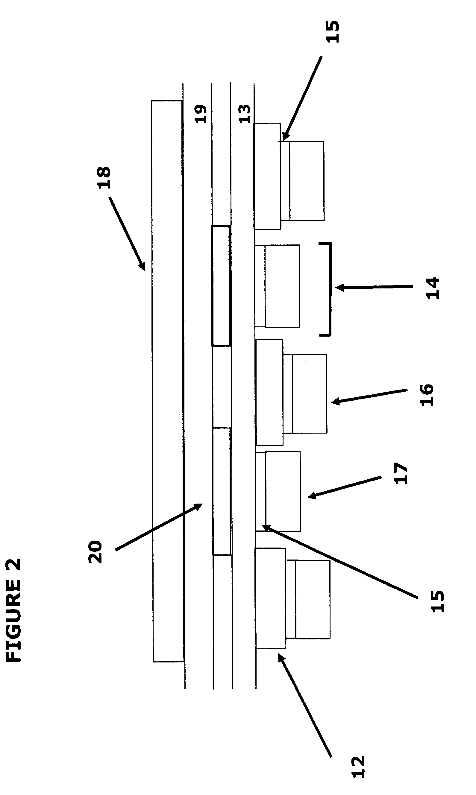
[0041]This exemplary OLED detector comprises a PIN-type device, with a semi-transparent contact deposited on the p-layer. The first layer deposited may be the semitransparent contact, for example ITO. The layer is deposited using, for example, sputtering in Ar atmosphere from appropriate ITO targets. This layer is followed by the deposition of a buffer layer, for example, zinc oxide (ZnO), whose function is to prevent interaction between the ITO layer and the following p-layer. The thin ZnO layer, which may be doped, for example with aluminum, is deposited using sputtering. The p-layer is deposited on the ZnO layer using PECVD techniques, using either RF glow discharge techniques, or ECR deposition techniques. The gases used for depositing the p-layer, which is made from an amorphous silicon-carbon alloy, are silane, hydrogen, methane, helium, and diborane, with diborane serving as the dopant. The ratio of methane to silane is...


PUM

PropertyMeasurementUnit
thicknessaaaaaaaaaa
thicknessaaaaaaaaaa
thicknessaaaaaaaaaa

Abstract

Integrated photoluminescence (PL)-based chemical and biological sensors are provided comprising a photodetector (PD), a long-pass filter, an excitation source, and a sensing element, all based on thin films or structures. In one embodiment the light source is an organic light emitting device (OLED) and the sensing element is based on thin films or solutions in microfluidic channels or wells. The PD and optical filters are based on thin film amorphous or nanocrystalline silicon and related materials. In another embodiment, sensor components are fabricated on transparent substrates, which are attached back-to-back to generate a compact, integrated structure.

Description

[0001]This application claims the benefit of U.S. Provisional Application Ser. No. 60 / 670,248 filed on Apr. 12, 2005, the entire disclosure of which is incorporated herein by reference.GOVERNMENT RIGHTS[0002]The United States Government has certain rights in this invention pursuant to Contract Number ECS0428220 between the National Science Foundation and Iowa State University.FIELD OF THE INVENTION[0003]The present invention relates to luminescent chemical and biological sensors having structural integration of sensor components.BACKGROUND OF THE INVENTION[0004]Detection and quantification of analytes are of prime interest in medical, biochemical, analytical chemical, occupational safety, microelectronic, environmental, military, and forensic applications. Electrochemical sensors can be used for these applications. However, electrochemical sensors consume analytes, have long response times, are limited with regard to in vivo use, and are susceptible to poisoning by various contamina...

Claims


Application Information

Patent Timeline
Patent Type & Authority Patents(United States)
IPC IPC(8): G01N21/64F21V9/16G01N21/00G01N21/76G02B6/00
CPCG01N21/6454B01L3/5027G01N2201/0628
Inventor SHINAR, RUTHSHINAR, JOSEPHDALAL, VIKRAM L.
Owner IOWA STATE UNIV RES FOUND
Why Eureka
Try Eureka