

Electronic device, dielectric ceramic composition and the production method
a technology of dielectric ceramic and dielectric device, which is applied in the direction of fixed capacitors, electrical apparatus, domestic applications, etc., can solve the problems of low specific permittivity of dielectric ceramic composition described in the article, unable to respond to downsizing and obtaining of a larger capacity, and liable to have little flexibility to obtain characteristics according to application, so as to achieve high specific permittivity
- Summary
- Abstract
- Description
- Claims
- Application Information
AI Technical Summary
Benefits of technology
Problems solved by technology
Method used
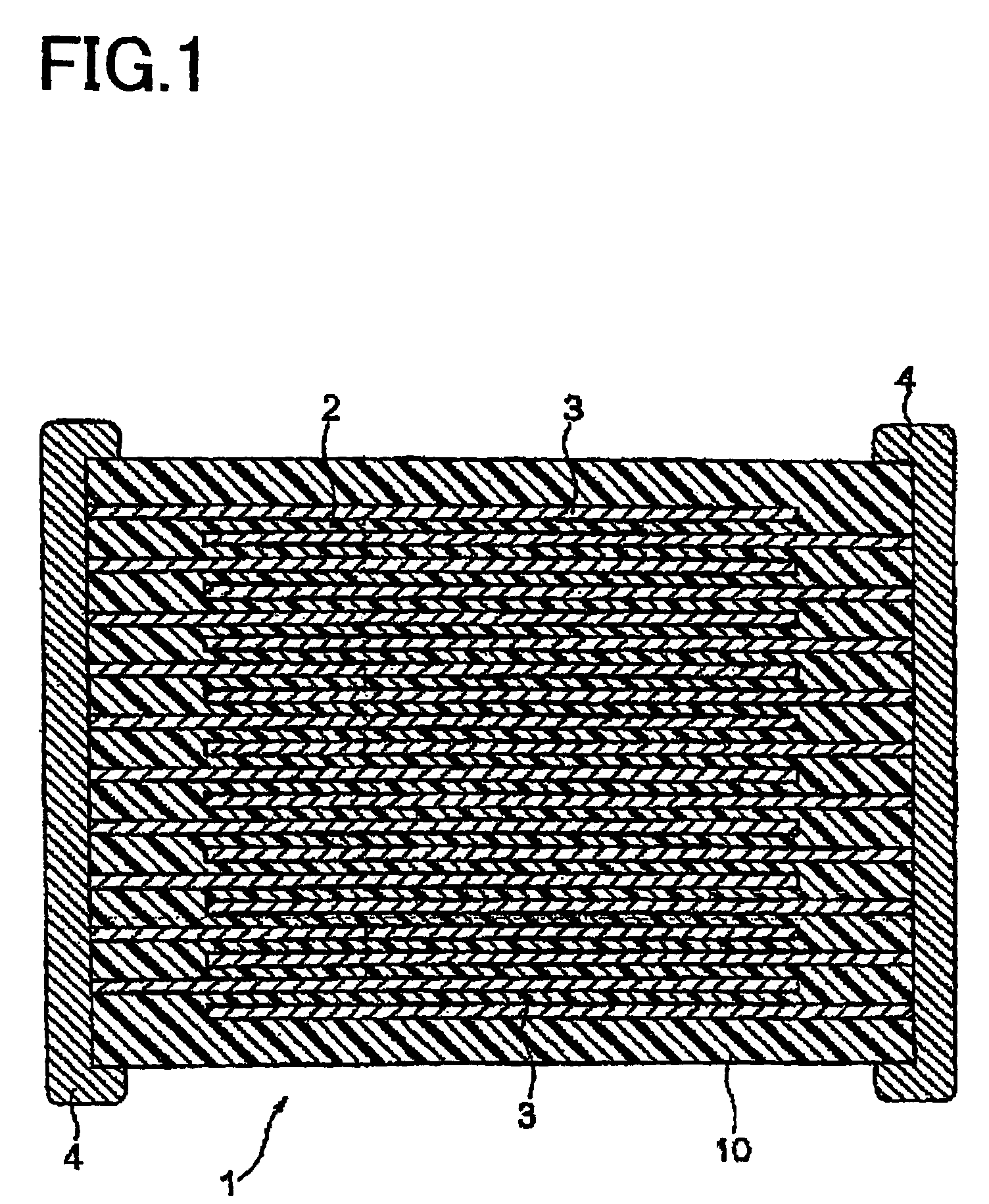
Image

Examples
example 1
[0158]First, BaTiO3 and CaTiO3 powders having an average particle diameter of 0.30 μm as the main component material and Y2O3 powder as the fourth subcomponent material to be reacted in advance (pre-added material) were prepared. Next, the prepared main component powders and a part of Y2O3 powder were weighed to obtain respective amounts shown in Table 1, wet mixed / pulverized by a ball mill to obtain slurry. After drying the slurry, calcination and pulverizing were performed, so that a post-reaction material was obtained. Note that the calcination condition was the temperature raising rate of 200° C. / hour, the holding temperature of 500° C., the temperature holding time of two hours and an atmosphere in the air. Namely, in the sample 1, only BaTiO3 powder was used as the main component material. An amount of Y2O3 to be reacted in advance was 0.1 mole in terms of Y atom (0.05 mole in terms of Y2O3) with respect to 100 moles of the main component (note that an amount of Y2O3 will be i...
example 2
[0185]As with sample 1, only BaTiO3 powder was used as the main component material, and Y2O3 (the fourth (a) subcomponent) was used as a material to be reacted in advance. Also, except for changing an amount of Y2O3 (the fourth (a) subcomponent) reacted in advance with the main component material to a value shown in Table 2 in terms of Y atom and amounts of Y2O3 (the fourth (a) subcomponent) and Gd2O3 (the fourth (b) subcomponent) added to the post-reaction material to values shown in Table 2 in terms of Y atom and Gd atom, each capacitor sample was obtained as with sample 1. The obtained respective samples were evaluated in the same way as in the example 1. The results are shown in Table 2.
[0186]Note that the ratio M2 / M1 between number of moles M1 of R1 of the fourth (a) subcomponent (pre-adding 0.05 mole and post-added 0.55 mole=0.6 mole) and number of moles M2 of R2 of the fourth (b) subcomponent (0.05 mole) in the finally-obtained dielectric ceramic composition was 0.08 in the e...
example 3
[0190]As with sample 1, only BaTiO3 powder was used as the main component material, and Yb2O3 (the fourth (a) subcomponent) was used instead of Y2O3 (the fourth (a) subcomponent) as a material to be reacted in advance. Also, except for changing an amount of Yb2O3 (the fourth (a) subcomponent) reacted in advance with the main component material and amounts of Y2O3 (the fourth (a) subcomponent) and Gd2O3 (the fourth (b) subcomponent) added to the post-reaction material to values shown in Table 3 in terms of R1 and R2 respectively, each capacitor sample was obtained as with the example 1. The obtained respective samples were evaluated in the same way as in the example 1. The results are shown in Table 3.
[0191]Note that the ratio M2 / M1 between number of moles M1 of R1 of the fourth (a) subcomponent and number of moles M2 of R2 of the fourth (b) subcomponent in the finally-obtained dielectric ceramic composition was 0.08 in the example 3.
[0192]
TABLE 3SubcomponentTemper-MainPre-addingPost...
PUM
| Property | Measurement | Unit |
|---|---|---|
| ionic radius | aaaaa | aaaaa |
| ionic radius | aaaaa | aaaaa |
| average crystal grain diameter | aaaaa | aaaaa |
Abstract
Description
Claims
Application Information