Polycrystalline dielectric thin film and capacitance element

a polycrystalline dielectric and capacitance element technology, applied in the direction of thin/thick film capacitors, fixed capacitors, ceramics, etc., can solve the problems of limited thinning of dielectric layers made by sheet methods, difficult industrial use, and inability of ceramic capacitors to maintain dielectric properties, etc., to achieve high specific permittivity

Active Publication Date: 2019-12-31
TDK CORPARATION
View PDF5 Cites 0 Cited by
  • Summary
  • Abstract
  • Description
  • Claims
  • Application Information

AI Technical Summary

Benefits of technology

[0006]The present invention is attainted in view of such circumstances, and the object is to provide the polycrystalline dielectric thin film and the capacitance element having high specific permittivity.
[0026]The polycrystalline dielectric thin film according to the present invention has the above mentioned characteristics, thereby attains extremely high specific permittivity of several thousands to several millions or larger when a frequency is around 1 MHz.

Problems solved by technology

However, the ceramic capacitor cannot maintain a dielectric property when a voltage having a resonance frequency or more is applied.
However, there is a limit to the thinning of the dielectric layer made by the sheet method.
However, the thin film capacitor disclosed in the patent document 1 needs a special single crystal substrate in order to carry out the epitaxial growth, thus an industrial use is difficult.

Method used


Image

  • Polycrystalline dielectric thin film and capacitance element
  • Polycrystalline dielectric thin film and capacitance element
  • Polycrystalline dielectric thin film and capacitance element

Examples


first embodiment

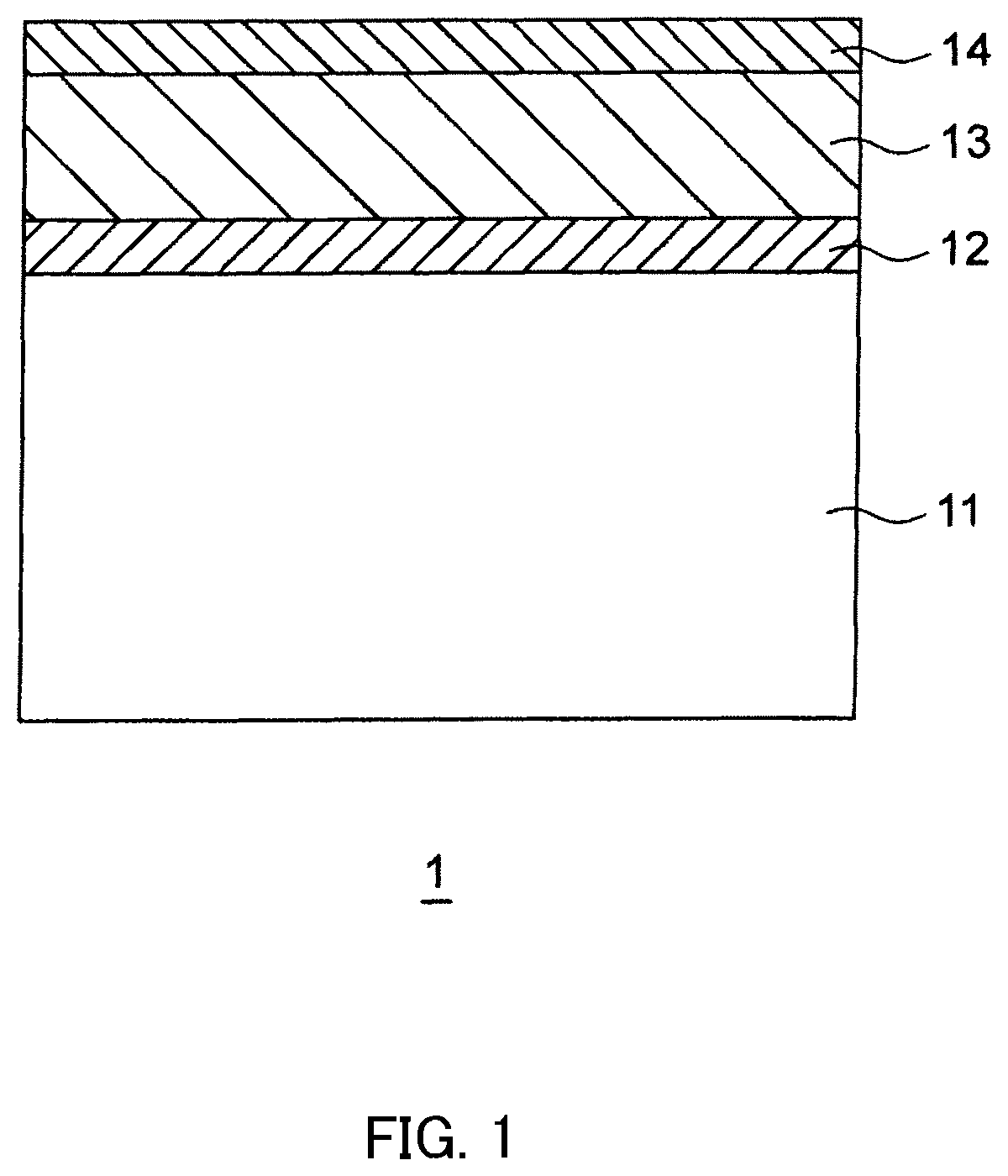
[0035]A schematic diagram of the thin film capacitor according to the present embodiment is shown in FIG. 1. The thin film capacitor 1 shown in FIG. 1 has a lower electrode 12 and a polycrystalline dielectric thin film 13 on a substrate 11 in this order, and also has an upper electrode 14 on the surface of the polycrystalline dielectric thin film 13.

[0036]The material of the substrate 11 is not particularly limited, but Si single crystal is used as the substrate 11 because of the cost and because it is easy to obtain. In case flexibility is important, Ni foil or Cu foil can be used as the substrate.

[0037]The material of the lower electrode 12 and the upper electrode 14 are not particularly limited as long as these function as the electrode. For example, Pt, Ag, and Ni or so may be mentioned. The thickness of the lower electrode 12 is preferably 0.01 to 10 μm. The thickness of the upper electrode 14 is preferably 0.01 to 10 μm.

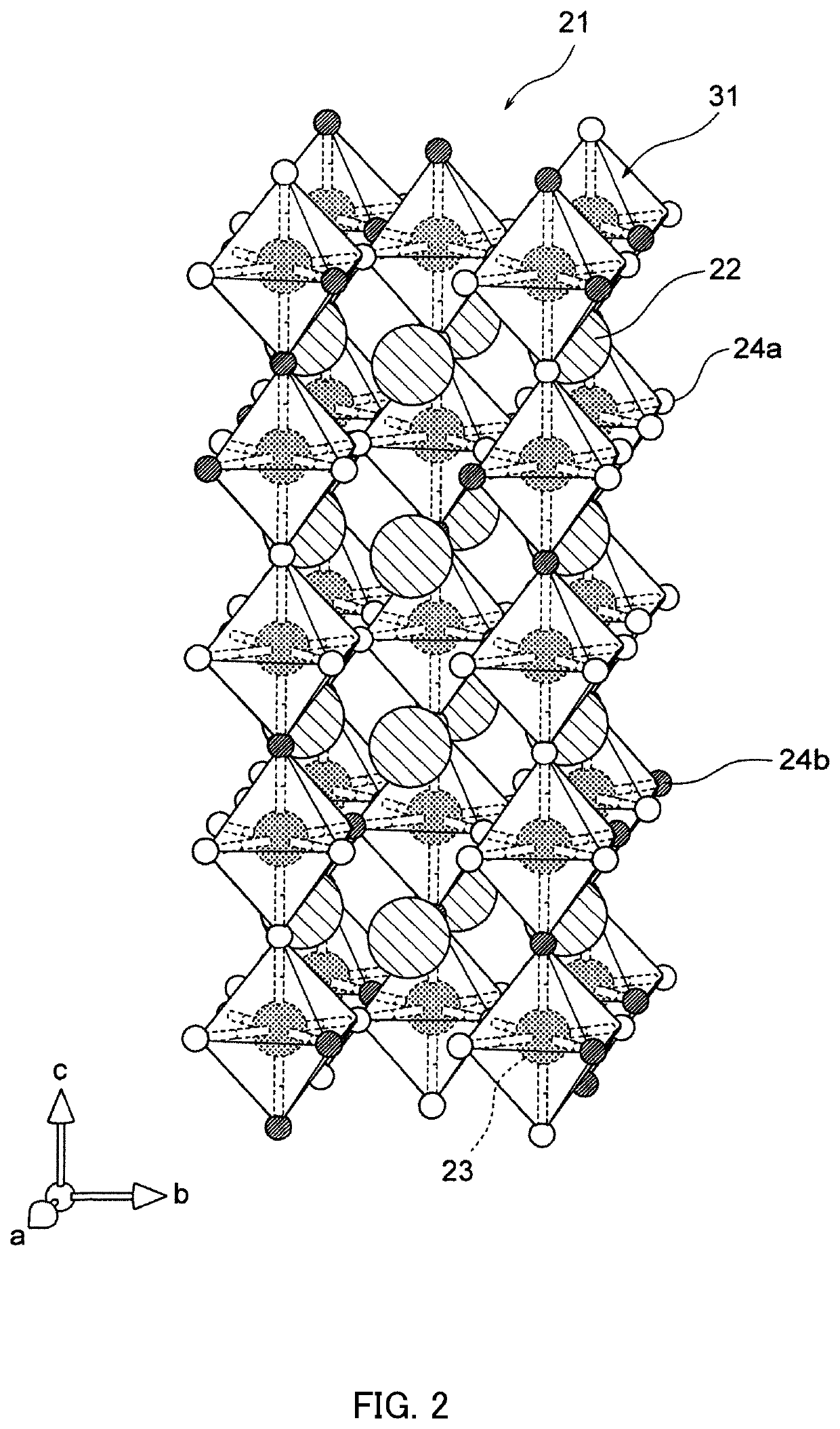
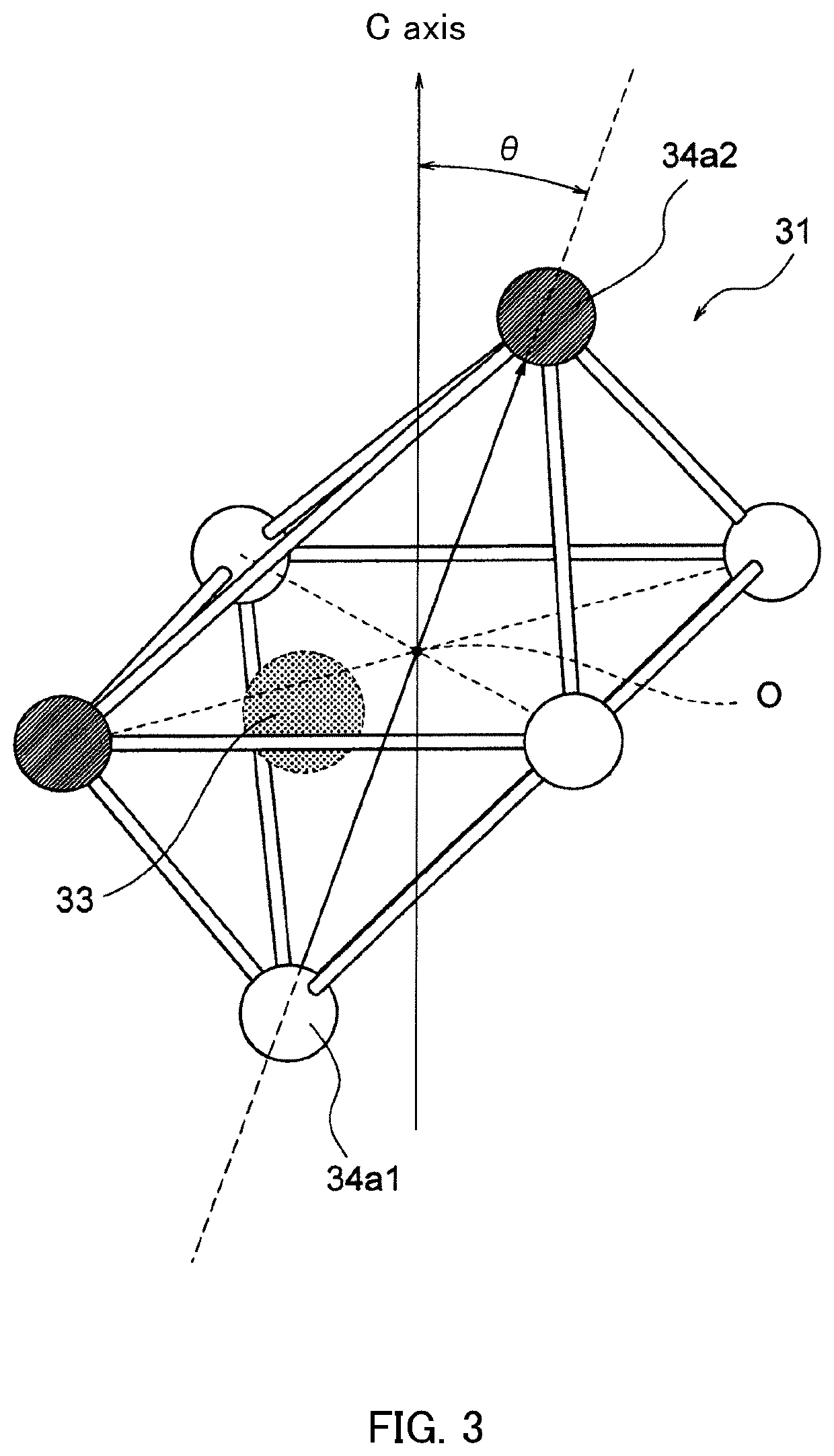
[0038]The polycrystalline dielectric layer has the main c...

second embodiment

[0074]The shape of the thin film capacitor according to the present embodiment is same as the first embodiment. The material of the substrate 11, the lower electrode 12, and the upper electrode 14 are same as the first embodiment. Further, the thickness of the lower electrode 12 is same as the first embodiment.

[0075]The polycrystalline dielectric thin film 13 comprises a main component made of an oxynitride expressed by a general formula of (Sr1-xBax)(Ta1-yNby)(O1-zNz)3, and 0.02≤x≤0.8, 0≤y≤0.4, and 0.033≤z≤0.233 are satisfied. Further, said oxynitride is the perovskite type oxynitride.

[0076]The polycrystalline dielectric thin film 13 according to the present embodiment can significantly improve the specific permittivity by having above mentioned oxynitride as the main component. Particularly, the specific permittivity is significantly improved in wide range of frequency of 1 kHz to 1 MHz, compared to the case of which the main component is made of oxide of barium titanate, and oxid...

example

[0080]Hereinafter, the present invention will be described based on further detailed examples, but the present invention is not to be limited thereto.


PUM

PropertyMeasurementUnit
thicknessaaaaaaaaaa
frequencyaaaaaaaaaa
thicknessaaaaaaaaaa

Abstract

A polycrystalline dielectric thin film including a main component made of an oxynitride expressed by a general formula of (M(1)1-xM(2)x)(M(3)1-yM(4)y)(O1-zNz)3. 0≤x≤1, 0≤y≤1, and 0<z<⅓ are satisfied. A total sum of nominal valences of M(1), M(2), M(3), and M(4) is 14. A crystal structure of the oxynitride includes an octahedron structure including a center atom, two 4a site atoms, and four 8h site atoms. The center atom is M(3) or M(4). The 4a site atom is O atom or N atom. The 8h site atom is O atom or N atom. An angle θ formed between a straight line connecting two 4a site atoms and a c-axis direction of the crystal structure in the octahedron structure satisfies 0.5°≤θ≤12°.

Description

BACKGROUND OF THE INVENTION1. Field of the Invention[0001]The present invention relates to a polycrystalline dielectric thin film and a capacitance element.2. Description of the Related Art[0002]Recently, a faster speed and higher capacitance are demanded for a wireless communication device such as a smart phone. Many ceramic capacitors are used for IC part of the smart phone. However, the ceramic capacitor cannot maintain a dielectric property when a voltage having a resonance frequency or more is applied. Therefore, the capacitor which can correspond to a higher frequency is demanded.[0003]In order to obtain the capacitor which can correspond to a high frequency, generally a capacitance of the capacitor needs to be improved. Further, the capacitor has a smaller size and a larger capacity by thinning and stacking a dielectric layer of the capacitor. In order to attain a thinned and multilayered capacitor, a sheet method has been widely used conventionally. However, there is a limit...

Claims


Application Information

Patent Timeline
Patent Type & Authority Patents(United States)
IPC IPC(8): C04B35/64C04B35/634C04B35/626C04B35/495H01G4/12
CPCC04B35/6262C04B35/63416C04B35/62655C04B35/495H01G4/1254C04B35/64C04B35/6264C04B2235/6567C04B2235/3895C04B2235/602C04B2235/606H01G4/08H01G4/10H01G4/33H01G4/085H01G4/1209H01G4/1227H01G4/1272H01L28/55C04B2235/3213C04B2235/3215C04B2235/3251C04B2235/77C04B35/465H01B3/12
Inventor UMEDA, YUJIYAMAZAKI, KUMIKO
Owner TDK CORPARATION
Why Eureka
Try Eureka