Maskless lithography system and method using optical signals

a lithography system and optical signal technology, applied in the field of maskless lithography system, can solve the problems of high cost of mask manufacturing, low through-put of masks, and low spatial arrangement of substrates, and achieve the effect of facilitating electro-optical data transmission

Inactive Publication Date: 2010-06-01
FRAUNHOFER GESELLSCHAFT ZUR FOERDERUNG DER ANGEWANDTEN FORSCHUNG EV
View PDF14 Cites 1 Cited by
  • Summary
  • Abstract
  • Description
  • Claims
  • Application Information

AI Technical Summary

Benefits of technology

[0007]It is an object of the present invention to provide a lithography system having an addressable pattern generation system and having a data transmission system which enables even highest data rates to be transmitted reliably to the inside of the vacuum chamber, and in particular in which no mechanical strain on the pattern generating system due to contacts or any space related problems occur. It is an additional object to provide simple allocation of the transferred data to the addressable individual elements in the pattern generating system. It is a further object for the data transmission system according to the present invention to be robust in terms of operation and to allow easy assembly and disassembly.
[0009]Such an arrangement facilitates both the transformation of the high data rate to be transmitted into the efficient optical range as well as the data transfer in a free beam connection system, which date transfer is not dependent on wiring (data lines). The opto-electrical data transmission system in the lithography system permits keeping the pattern generating system free from cumbersome wire-bound and mechanically straining connections to the outside, and thus enables relief from mechanical strain. Therefore, upon assembling or maintaining the lithography system, cumbersome wired connections for data transmission do not need to be made or removed directly at the pattern generating system. In the present invention, the entire data transmission is based purely on optics and is independent of wiring, at least directly in front of the pattern generating system, owing to the integration of a free beam connection system. The opto-electrical data transmission system is very efficient, so that even the highest data rates can be transmitted. The electro-optically converted data are guided as parallel free beams directly to the pattern generating system, with the number of the parallel free beams being adapted to the data rate to be transmitted via the predetermined transmission rate of the electro-optical converters. Assuming an exemplary data rate of 10 Gbits / s per electro-optical converter, 256 parallel free beams are required for transmitting a data rate of 2.56 Tbit / s. These parallel free beams' paths are directed at the opto-electrical converters in the pattern generating system. From there, the data, which are converted into electrical signals, are guided to the individual elements of the pattern generating system via subsequent signal processing. In an exemplary embodiment, the opto-electrical converters in the pattern generating system accordingly detect the incoming optical data at their data rate of 10 Gbits / s. In the region of the free beams, which are independent of wiring, the light serving as the data carrier in the vacuum chamber is neither influenced by the high voltage present therein during structuring, nor by the particle beam, whose particles are usually ions or electrons. This has a great advantage in that the data can be optically irradiated directly onto the opto-electrical converter—accepting that their paths cross the particles' paths—without occurrence of any problems with respect to potentials. Space consuming and complex bundles of wiring and their mechanical contacting are not required.
[0012]According to a further embodiment of the present invention, the light exit locations may be disposed outside the vacuum chamber, and the free beams may be guided into the vacuum chamber through a light transparent window in the vacuum chamber. In this way, the data transmission to the inside of the vacuum chamber is already independent of wiring and achieved by free beams. The free beams are guided simply through a window, which is integrated into the wall of the vacuum chamber. When the light exit locations are positioned outside the vacuum chamber, space requirements and efforts associated with mounting the free beam connection system inside the vacuum chamber are reduced. No passage for any wiring for data transmission into the inside of the vacuum chamber is required, and a complete decoupling from the high vacuum and from the high voltage fields inside the vacuum chamber results. Deflection of the free beams, which enter the inside through the window, onto the opto-electrical converters is again readily achieved by optical deflection arrangements. Any suitable deflector may be used. In order to save space outside the vacuum chamber also, a further embodiment of the present invention provides that the light exit locations are disposed directly at the window from the outside. Thereby, a series of further constructional simplifications may result, which are discussed further below. In addition, the light exit locations may advantageously be disposed orthogonally below the window, and the free beams may be guided via an additional optical deflection arrangement through the window into the inside of the vacuum chamber. Thus, deflection arrangements may also be provided outside the vacuum chamber in order to be able to guide the free beams in an optimal space saving manner. Finally, according to a further embodiment of the present invention, the window may also be recessed into the vacuum chamber. This enables a space saving positioning of the light exit locations on the outside, but still within the region of the vacuum chamber. Furthermore, predetermined optical distances may be met more easily. This is described in more detail later on in the general description and the exemplary embodiments. In order to avoid interfering influences due to stray light and other effects, when free beams are irradiated from external light exit locations through the window, it is particularly advantageous if the window is provided with a cover shielding against external light and electromagnetic fields in a region outside of the passing free beams. The covers may be simple mechanical or optical covers. Furthermore, the free beams may be grouped into arrays, which are locally precisely defined and whose surrounding is therefore easier to cover.
[0015]If the light exit locations are configured to be active, a further embodiment of the present invention advantageously provides that the electro-optical converters as light exit locations are configured as emitting lasers. Thus, electro-optical conversion of the pattern data occurs only directly at the light exit location. Providing a wire-unbound feed line to the emitting laser does not cause any problems, in particular if the feed line is disposed outside the vacuum chamber. Active light entry locations may also be realized by configuring the opto-electrical converters as light entry locations formed by photodiodes, according to a further embodiment of the present invention. The data are opto-electrically converted directly in the light entry locations and passed on in a wire-bound system. In an embodiment comprising active emitting elements (for instance emitting lasers) and active receiving elements (for instance photodiodes), no light waveguides are required, which results in a particularly compact embodiment. Other active components may also be used. The opto-electrical converters formed by photo diodes require less than 50 micrometers of space, for instance. Assuming a distance between the individual photo diodes in a range of 250 micrometers to 500 micrometers, for transmitting a sum data rate of 2.56 Tb / s by 256 parallel light waveguides and thus 256 photodiodes arranged in a row, each of which is used for addressing a group of individual elements (apertures), a space requirement for the diode array in the one direction of between 64 mm and 128 mm results. Such a band-shaped diode array may be disposed on the so called “blanking plate”, which holds programmable chips comprising the individual apertures, in a known lithography system. Such a programmable aperture system is known, for instance, from the abstract of the publication “Programmable Aperture Plate for Maskless High Throughput Nanolithography”, by I. L. Berry, et al.; (Journal of Vacuum Science and Technology, B, 1997, Volume 15, No. 6, pages 2382 to 2386). A particular advantage of the lithography system according to the present invention, however, lies in the option that light beams and particle beams may cross one another in the vacuum chamber, and that therefore, there is the option of a free choice of arrangement and accessibility of the opto-electrical converters. That way, particularly space saving arrangements may be realized. Furthermore, major advantages result from the speed of data transmission of the blanking plate, since shorter distances may be realized. According to a further embodiment of the lithography system according to the present invention, it is therefore advantageous if the opto-electrical converter is disposed directly in the pattern generating system. Accessibility of the converters via the free space distance in the vacuum chamber is always granted. Complex, sensitive and obstructing wiring, which is also critical with respect to achievable data speeds, is not required. In exemplary embodiments, the pattern generating system can be configured as a programmable aperture plate system, and the photodiodes may thus be distributed over the blanking plate and may be allocated there to groups of apertures via multiplex elements, whereby a major simplification of the arrangement and spacing savings can be achieved.
[0017]The present invention can facilitate electro-optical data transmission into and from a closed, badly accessible space having extreme conditions on its inside using a free beam connection system. Additionally, it is, however, possible—at least for relatively small amounts of energy—to realize an optical transmission of energy into the inside of the vacuum chamber without use of wires, in order to induce a process in the vacuum chamber, for instance, such as a switching process, to generate an electrostatic field or to charge up an energy storage. According to a further embodiment of the present invention, an optical energy transmission onto the addressable pattern generating system may be advantageously carried out using the opto-electrical free beam connection system.

Problems solved by technology

It has, however, also a disadvantage because of the extremely expensive manufacturing of the masks which can only be balanced by mass production of circuit layouts, because of the transfer of errors in the mask and because of the rather complex alignment when the mask is brought into position.
However, this method has the disadvantage of a relatively low through-put of substrates as a result of the slow, serial structuring process employing the particle beam.
The data rate, which needs to be processed in this preferred concept and which comprises the data for addressing the digitized structure pattern having 600,000 mask points, for instance, which are usually irradiated several times (grey scale system, comparable to the principle of the ink jet printer), and the addressing of the mounting table, is extremely high, and easily reaches several Tbit / s, such that suitable transmission of the data rate to the pattern generating system inside the vacuum chamber of the lithography system constitutes a particular problem associated with the direct structuring technique.
Thus, problems arise with the respect to their spatial arrangement and allocation, and in particular with respect to the mechanical fixation of the data lines to the carrier plate of the individual element to be addressed.
Furthermore, removing the data lines for purposes of maintenance in the vacuum chamber is very complex.
In addition, negative effects on the data to be transmitted may occur due to the conditions inside the vacuum chamber, in particular due to the applied high voltage.
Therefore, upon assembling or maintaining the lithography system, cumbersome wired connections for data transmission do not need to be made or removed directly at the pattern generating system.
Furthermore, the light exit locations of the free beam connection system inside the vacuum chamber may be disposed at a greater distance from the pattern generating system, which results in a lengthening of the distance covered by the free beams.
Upon assembly, maintenance or even during operation, undesired changes of adjustment may occur due to mechanical tolerances and changes of shape, both upon alignment of the beam as well as at the location of the detector or converter, respectively.

Method used


Image

  • Maskless lithography system and method using optical signals
  • Maskless lithography system and method using optical signals
  • Maskless lithography system and method using optical signals

Examples


Embodiment Construction

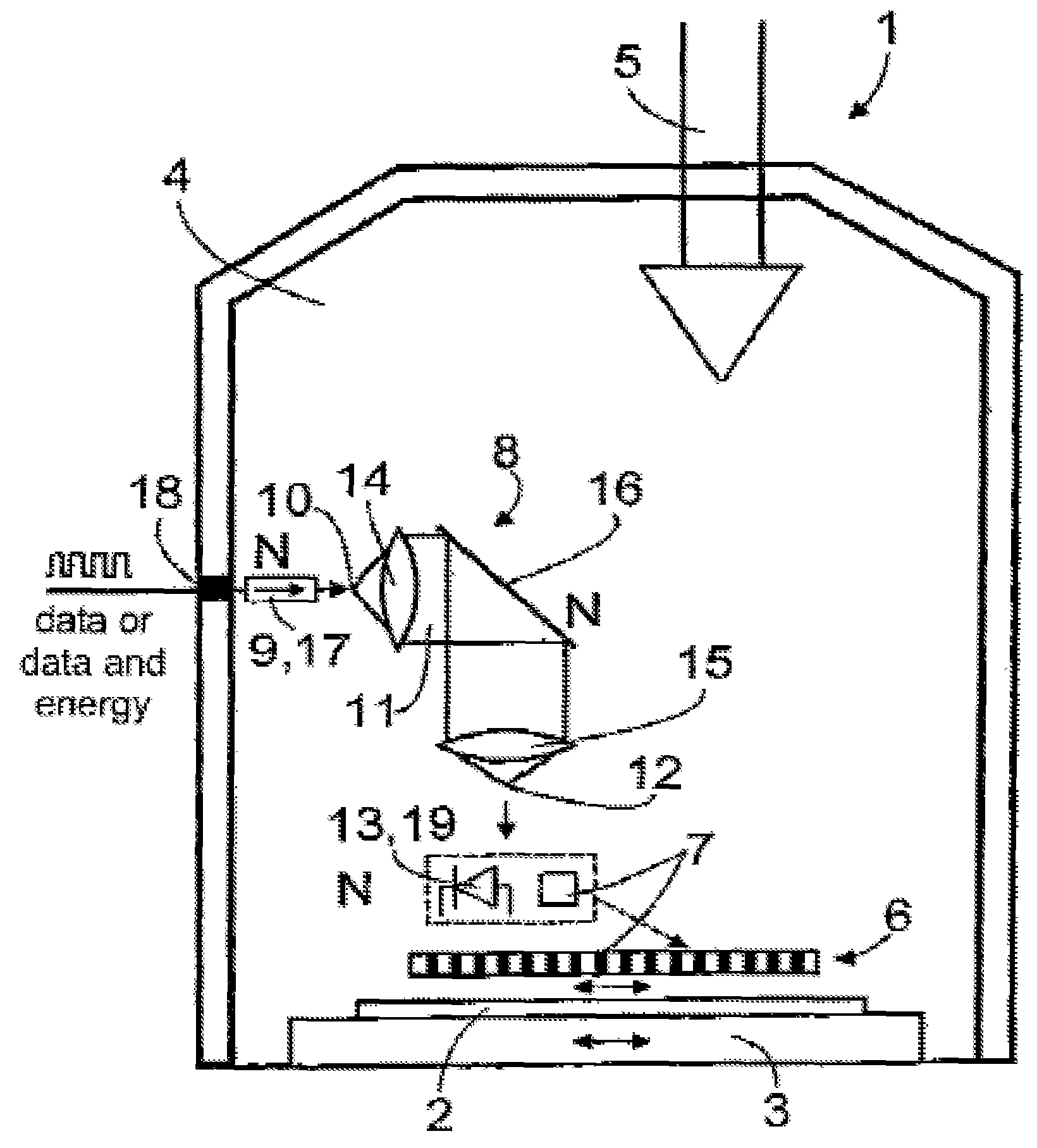
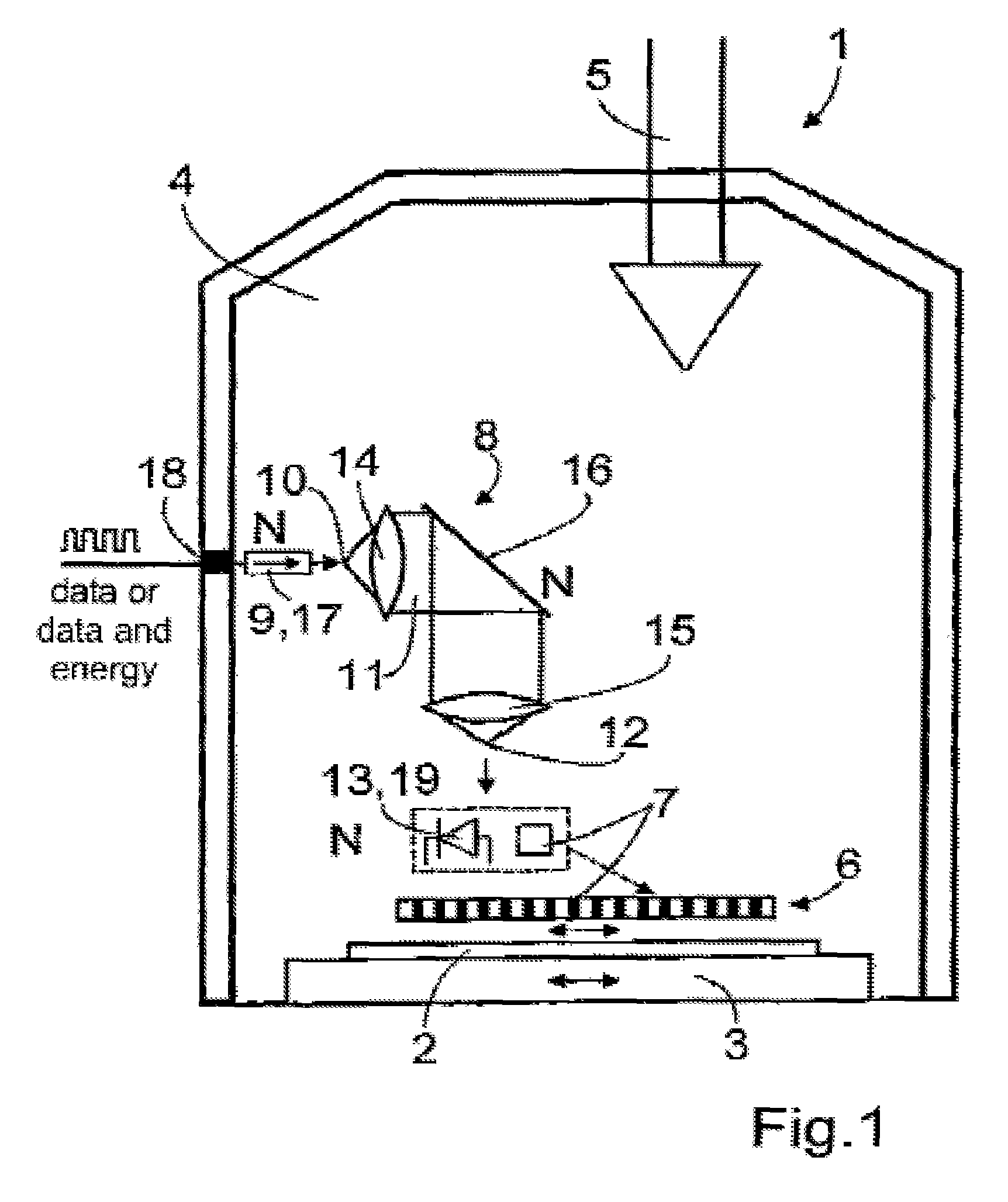
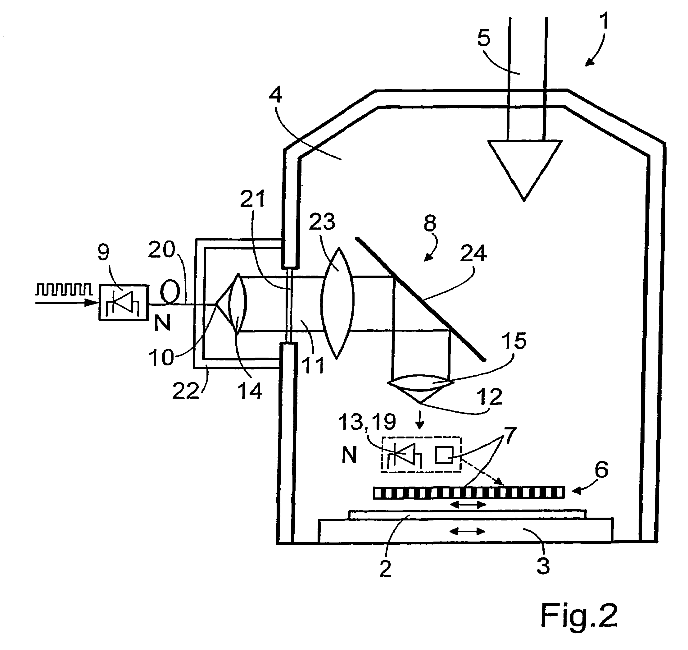
[0029]FIG. 1 schematically shows a section of a maskless lithography system 1 according to the present invention for direct, nano-scaleable structuring of a substrate 2, for instance a wafer made of silicon, which is disposed on a moveable mounting table 3. A cross-section of vacuum chamber 4 is depicted, the vacuum chamber 4 having a potential of 100 kV, for instance, on the inside. A homogeneous, broad particle beam 5, comprising electrons in this instance, is guided from the particle source, which is disposed in high vacuum, from the top into the vacuum chamber 4, wherein it is incident on an addressable pattern generating system 6 disposed above substrate 2. In the pattern generating system 6, which preferably is a programmable aperture plate system, a digital structuring pattern for irradiating substrate 2 with the particle beam 5 is generated with the assistance of a computer. To this effect, individually addressable apertures 7, which form the points of the structure or indiv...


PUM

PropertyMeasurementUnit
distancesaaaaaaaaaa
distanceaaaaaaaaaa
transmission wavelengthaaaaaaaaaa

Abstract

In a lithographic system, data transmission is carried out by a powerful electro-optical free-beam connection system enabling optical pattern data to be guided from light exit places to light entrance places inside the vacuum chamber by free-space optical beams in order to produce control signals. The burden on the pattern production system is significantly reduced by the disappearance of mechanical and electrical contacts. The paths of the free-space optical beams and the particle beams can intersect each other in a non-influential manner. Active photodiodes acting as light exit places can be spatially disposed directly in the pattern production system. Passive light waveguides which can be bundled together to form multipolar fibre array plugs, or active transmission lasers, either of which can also act as light exit places, can be arranged outside the vacuum chamber.

Description

[0001]This application is a continuation of International Patent Application No. PCT / DE2004 / 000924 filed Apr. 29, 2004, the publication of which by the International Bureau was not in the English language. This application also claims priority under 35 U.S.C. 119(d) to German Patent Application No. DE 103 19 154.2, filed Apr. 29, 2003. The entire contents of each of the above-identified applications are incorporated herein by reference.BACKGROUND[0002]1. Field of the Invention[0003]The present invention relates to a maskless lithography system for direct, nano-scale capable structuring of a substrate disposed on a movable mounting table in a vacuum chamber supplied with a high voltage, using a charged particle beam generated by a beam source, and an addressable digital pattern generating system onto which the structure pattern to be generated is transmitted as a set of pattern data generated with computer assistance using a data transmission system.[0004]2. Brief Description of Rela...

Claims


Application Information

Patent Timeline
Patent Type & Authority Patents(United States)
IPC IPC(8): G21K5/10G03F7/20
CPCG03F7/70991G03F7/70291
Inventor WALF, GODHARDKUHLOW, BERNDT
Owner FRAUNHOFER GESELLSCHAFT ZUR FOERDERUNG DER ANGEWANDTEN FORSCHUNG EV
Why Eureka
Try Eureka