Semiconductor memory device including a semiconductor film made of a material having a spontaneous polarization and method for fabricating the same
a semiconductor film and memory device technology, applied in the direction of semiconductor/solid-state device manufacturing, semiconductor devices, semiconductor devices, etc., can solve the problems of reducing the size of the capacitor, reducing the capacity of the capacitor, and the capacitor-type ferroelectric memory is unsuitable for an in-crease capacity. , to achieve the effect of improving retention characteristics, easy control of spontaneous polarization direction, and excellent sta
- Summary
- Abstract
- Description
- Claims
- Application Information
AI Technical Summary
Benefits of technology
Problems solved by technology
Method used
Image
Examples
embodiment 1
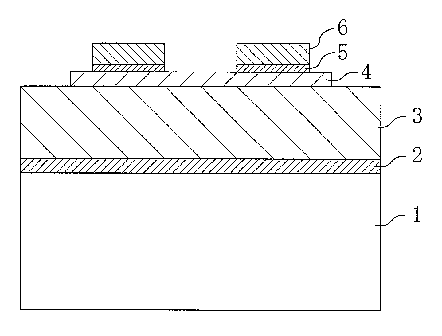
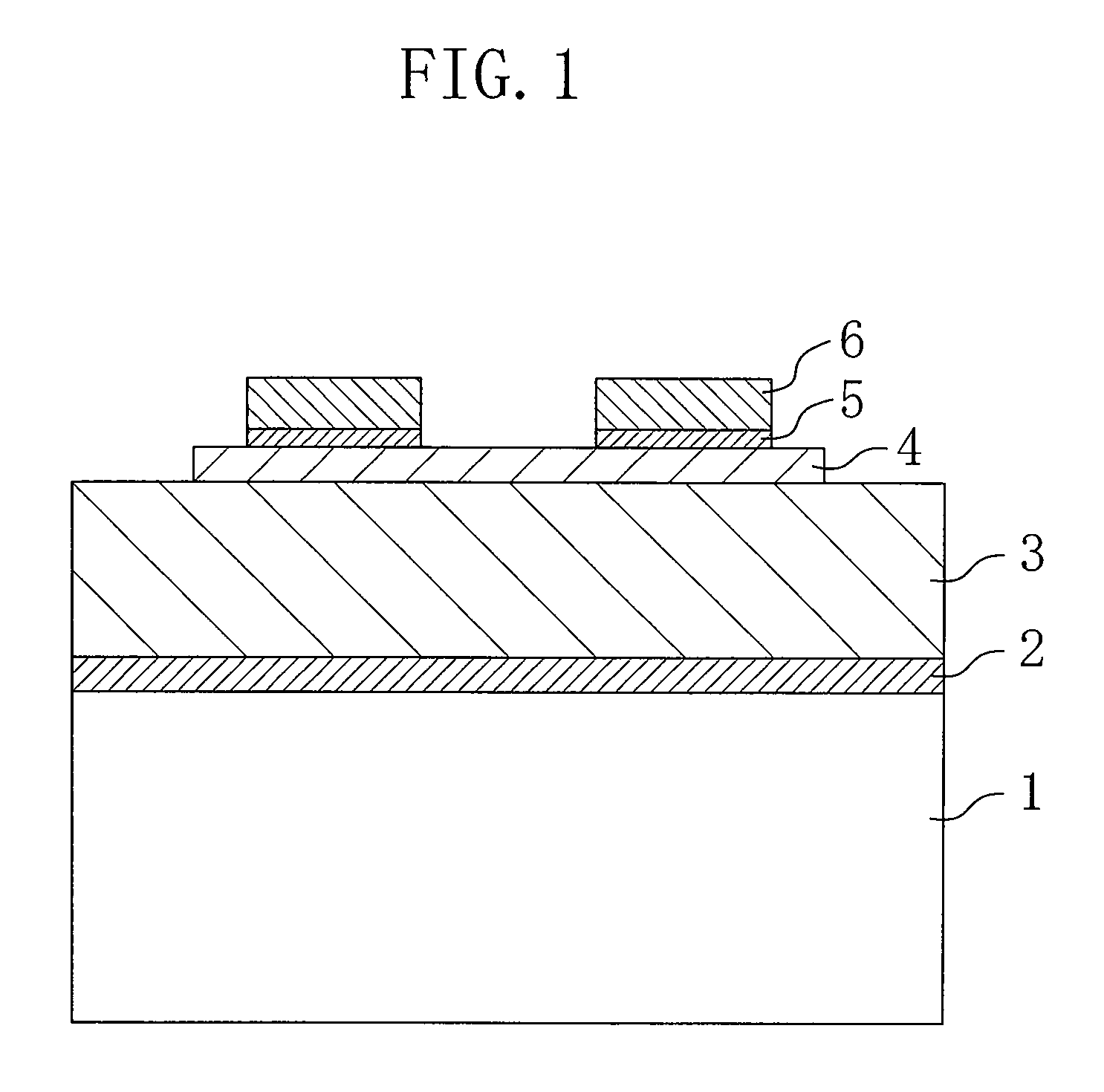
[0038]FIG. 1 is a cross-sectional view schematically showing a structure of a semiconductor memory device according to the first embodiment of the present invention.
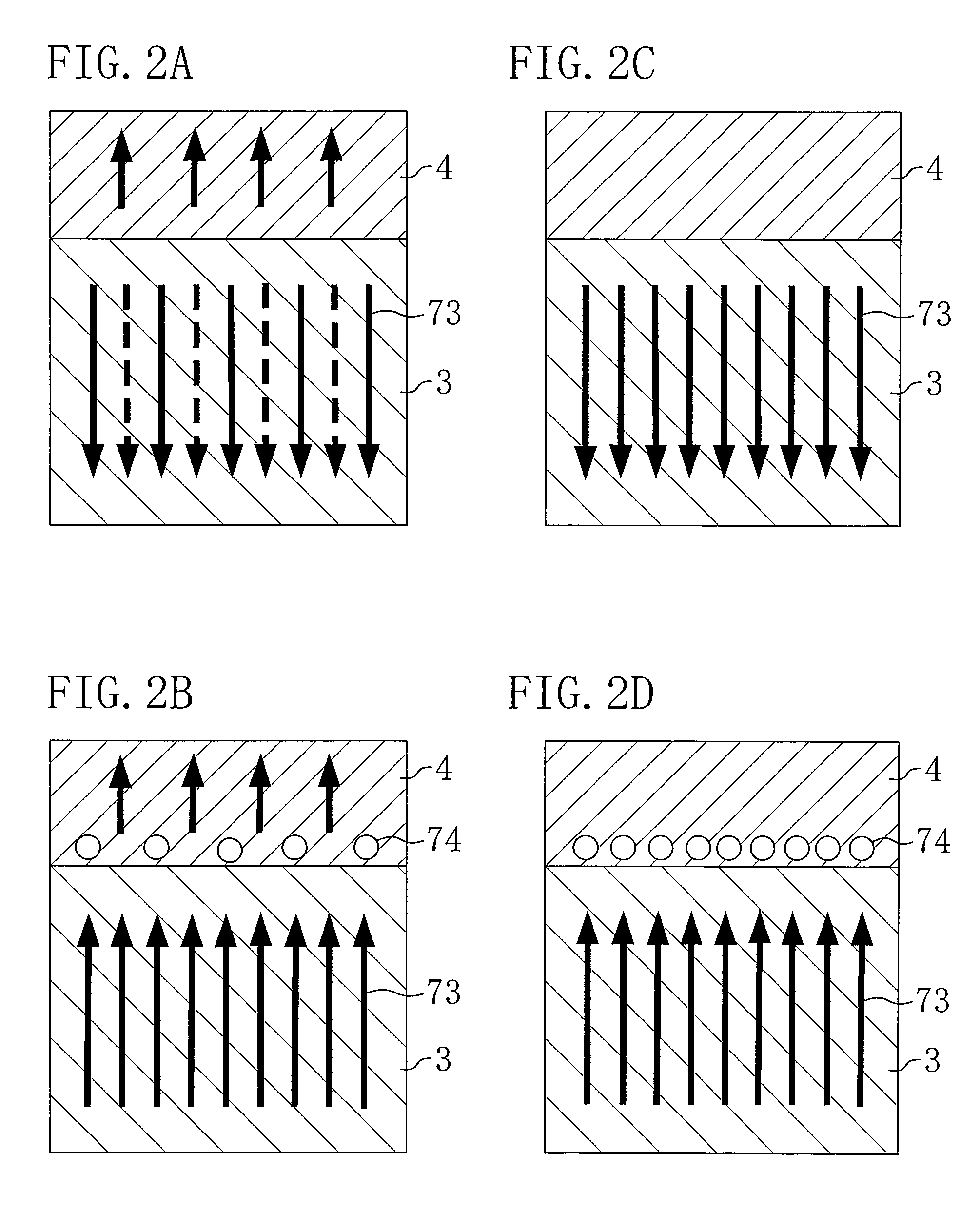
[0039]As shown in FIG. 1, the semiconductor memory device according to the present embodiment is composed of a field effect transistor using the interface between a ferroelectric film 3 and a semiconductor film 4 as a channel and comprising a gate electrode 2 to which a voltage for controlling the polarization state of the ferroelectric film 3 is applied and source / drain electrodes 5 and 6 for detecting a current flowing in the channel in accordance with the polarization state. The semiconductor film 4 is made of a material having a spontaneous polarization, in which the direction of the spontaneous polarization is parallel with the interface between the ferroelectric film 3 and the semiconductor film 4.
[0040]In the present embodiment, the semiconductor film 4 is composed of a ZnO film having a wurtzite-type crystal stru...
embodiment 2
[0063]In the first embodiment, the crystal orientation (the direction of spontaneous polarization) of the semiconductor film 4 is controlled by the crystal orientation of the ferroelectric film 3. However, to determine the crystal orientation of the ferroelectric film 3, it is necessary to use a substrate having a specified crystal structure and a specified crystal orientation. The second embodiment of the present invention provides a method for fabricating a semiconductor memory device comprising a semiconductor film having a crystal orientation thereof controlled in a predetermined direction without being restricted by the type of the substrate.
[0064]FIGS. 12A to 13D are step cross-sectional views schematically illustrating the method for fabricating the semiconductor memory device according to the present embodiment;
[0065]First, as shown in FIG. 12A, a MgZnO film 82 having a thickness of 20 nm and a ZnO film 83 having a thickness of 30 nm are continuously grown by a PLD method on...
PUM
 Abstract
Description
Claims
Application Information


