

Blocking dielectric engineered charge trapping memory cell with high speed erase
a memory cell and dielectric engine technology, applied in the field of flash memory technology, can solve the problems of limiting the ability to increase the density of flash memory, affecting the performance of flash memory, etc., and achieves the effects of fast erase, high electron barrier height, and fast programming
- Summary
- Abstract
- Description
- Claims
- Application Information
AI Technical Summary
Benefits of technology
Problems solved by technology
Method used
Image

Examples
Embodiment Construction
[0032]A detailed description of embodiments of the present invention is provided with reference to the FIGS. 1-11.
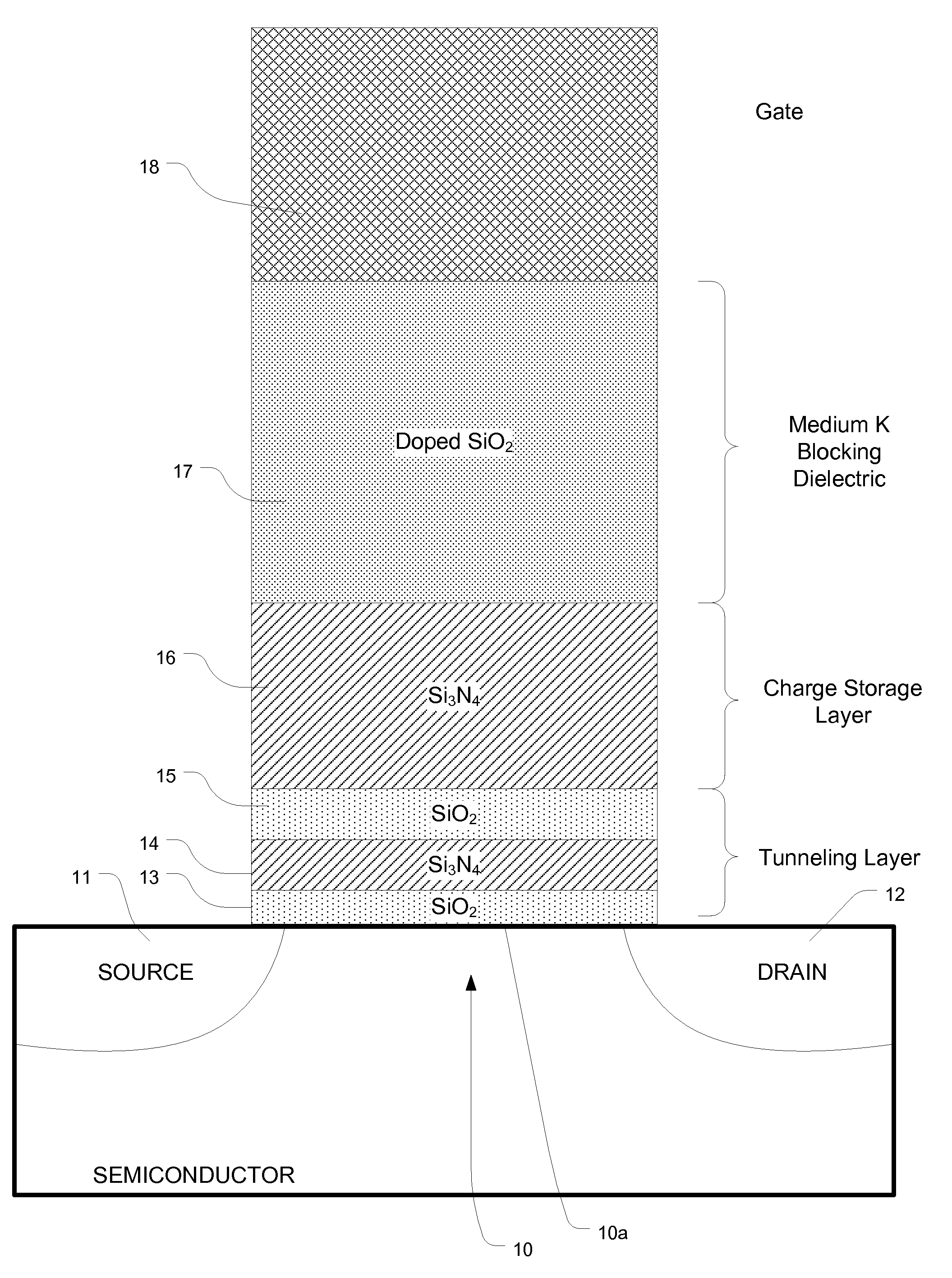
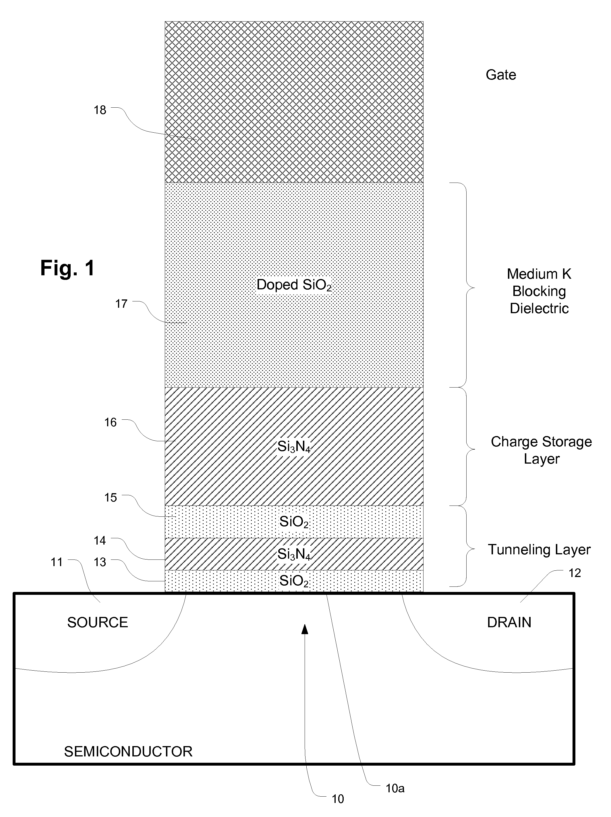
[0033]FIG. 1 is a simplified diagram of a charge trapping memory cell employing a medium κ blocking dielectric layer and a band gap engineered dielectric tunneling layer. The memory cell includes a channel 10 in a semiconductor body, and a source 11 and a drain 12 adjacent channel.
[0034]A gate 18 in this embodiment comprises p+ polysilicon. N+ polysilicon may also be used. Other embodiments employ metals, metal compounds or combinations of metals and metal compounds for the gate 18, such as platinum, tantalum nitride, metal silicides, aluminum or other metal or metal compound gate materials. For some applications, it is preferable to use materials having work functions higher than 4.5 eV. A variety of high work function materials suitable for use as a gate terminal are described in U.S. Pat. No. 6,912,163, referred to above. Such materials are typically deposited using s...
PUM
 Abstract
Description
Claims
Application Information