[0012]A blocking dielectric engineered, charge trapping memory
cell is described including a charge trapping element that is separated from one of a gate and a
semiconductor body including a channel by a blocking dielectric comprising a
metal doped
silicon oxide, such as aluminum doped
silicon oxide, and that is separated from the other of the
semiconductor body including the channel and the gate by a tunneling dielectric. The blocking
dielectric layer is engineered to have a dielectric constant κ greater than
silicon dioxide, and preferably in a range of about 4.5 to 7, and is paired with a gate material providing a relatively
high electron barrier height, such as greater than 2.5 eV. As discussed in detail below, the
electron barrier height and dielectric constant are tuned by selecting concentration of
metal in the
metal doped silicon oxide and by selecting a suitable gate material, to enable fast
programming and fast erase without erase saturation, with excellent reliability and retention characteristics. A process for manufacturing the memory cell is described, which includes forming the
metal doped silicon oxide layer as the blocking dielectric.
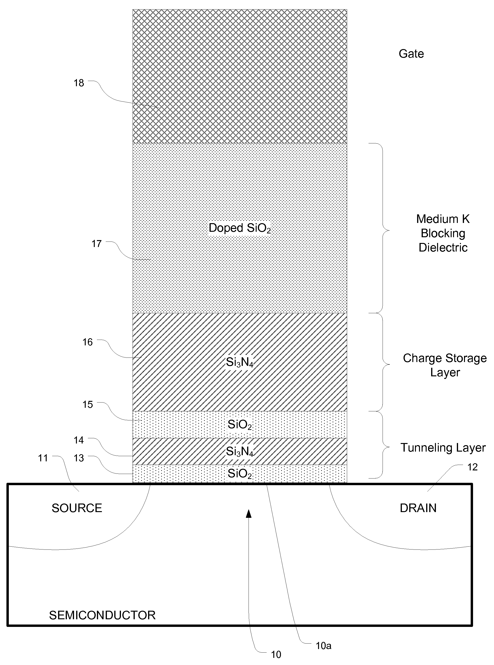
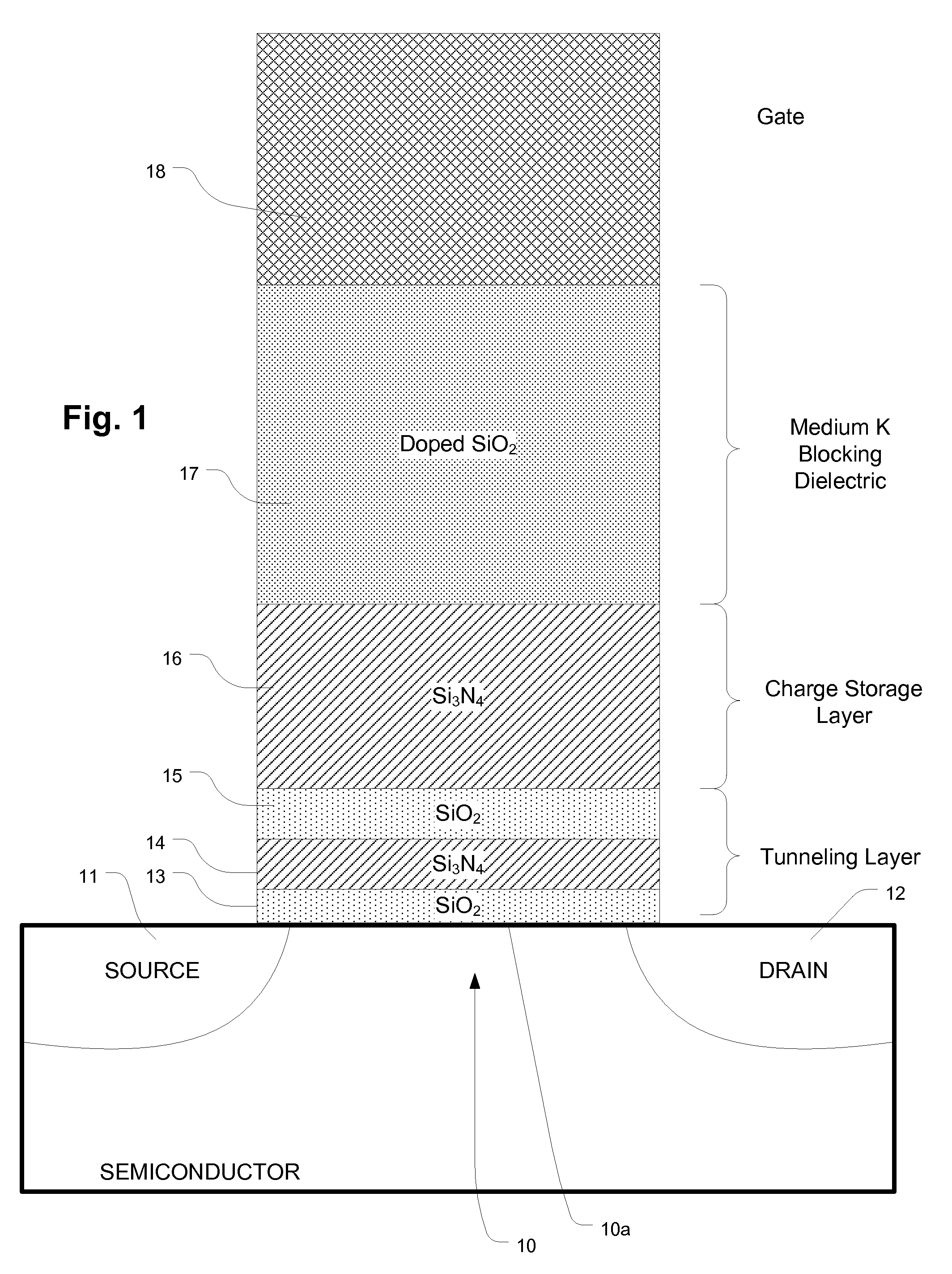
[0013]The technology is combined in the memory described here with a bandgap engineered tunneling dielectric that includes a combination of materials having negligible charge trapping efficiency, and
band offset characteristics. The bandgap engineered tunneling dielectric lowers the operating voltages required for the device, and enables the use of blocking dielectrics having a
medium range, compared to the prior art without significant tradeoffs in performance, while providing improved reliability. The
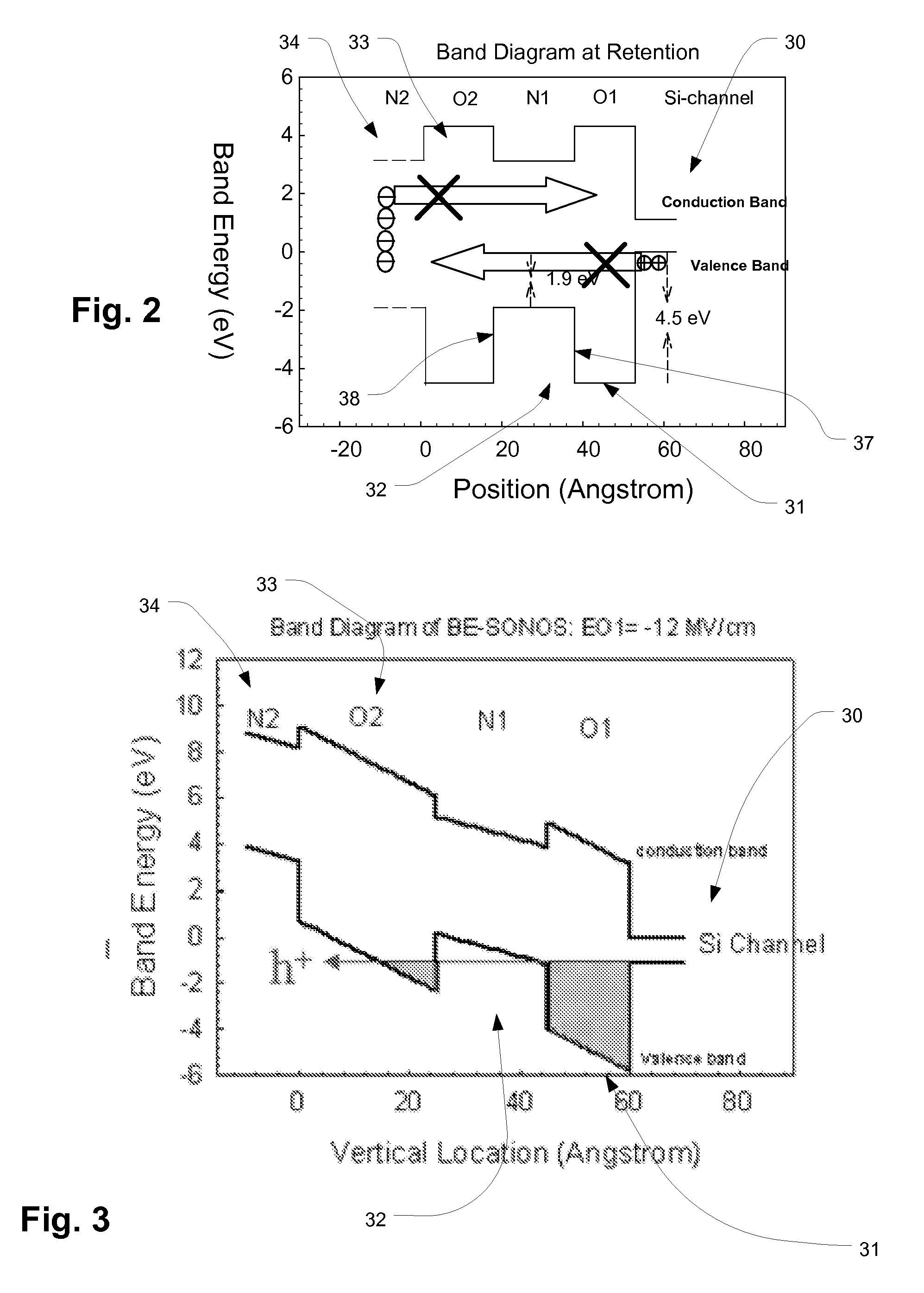
band offset characteristics include a relatively large hole tunneling barrier height in a thin region at the interface with the semiconductor body, and an increase in
valence band energy level so that the hole tunneling barrier height at a first offset less than 2 nm for example from the channel surface, from the interface is relatively low. The
band offset characteristics also include an increase in
conduction band energy by providing a
thin layer of relatively
high electron tunneling barrier height at a second offset more than 2 nm from the channel surface, separating the material with a relatively lower hole tunneling barrier height from the charge trapping layer.
[0014]The
valence band energy level at the first offset is such that an
electric field sufficient to induce hole tunneling through the thin region between the interface with the semiconductor body and the offset, is also sufficient to raise the
valence band energy level after the offset to a level that effectively eliminates the hole tunneling barrier in the engineered tunneling dielectric after the offset. This structure enables
electric field assisted hole tunneling at high speeds while effectively preventing charge leakage through the engineered tunneling dielectric in the absence of electric fields or in the presence of smaller electric fields induced for the purpose of other operations, such as reading data from the cell or
programming adjacent cells.
[0015]In a representative device, the engineered tunneling dielectric layer consists of an ultrathin silicon oxide layer O1 (e.g. <=15 A), an ultrathin
silicon nitride layer N1 (e.g. <=30 A) and an ultrathin silicon oxide layer O2 (e.g. <=30 A), which results in an increase in the valence band energy level of about 2.6 eV at an offset 15 A or less, from the interface with the semiconductor body. The O2 layer separates the N1 layer from the charge trapping layer, at a second offset (e.g. about 35 to 45 Å from the interface), by a region of lower valence band energy level (higher hole tunneling barrier) and higher
conduction band energy level. The electric field sufficient to induce hole tunneling between the interface and the first offset also raises the valence band energy level after the second offset to a level that effectively eliminates the hole tunneling barrier, because the second offset is at a greater distance from the interface. Therefore, the O2 layer does not significantly interfere with the electric field assisted hole tunneling, while improving the ability of the engineered tunneling dielectric to block leakage during low fields.
[0018]The present technology combines techniques for reducing the electric field in the blocking dielectric layer relative to the tunneling dielectric layer, with techniques for reducing the magnitude of the electric field required for erase to achieve high speed erase operations without saturation, enabling a large
memory window compared to prior devices. Also,
charge retention and endurance characteristics of the memory cell are very good.

