Electromagnetic wave detector with an optical coupling surface comprising lamellar patterns

Inactive Publication Date: 2010-06-22
THALES SA
View PDF28 Cites 0 Cited by
  • Summary
  • Abstract
  • Description
  • Claims
  • Application Information

AI Technical Summary

Benefits of technology

[0018]Advantageously, the etch depth may be around λ / 4 instead of λ / 2, according to the grating theory known by those skilled in the art and described for example in “Electromagnetic Theory of Gratings” by R. Petit, which shows that the etch depth in the case of a crossed (2D) grating must be twice that of a simple lamellar (1D) grating. From an industrial standpoint, reducing the thickness of the layers to be etched will allow the fabrication time and the fabrication costs to be reduced but will also increase the production.

Problems solved by technology

The major drawback of this type of matrix structure lies in the depth d for diffractive features that are generally produced within an encapsulation layer EL, thereby protecting the multiple quantum well MQW structure as illustrated in FIG. 3.

Method used


Image

  • Electromagnetic wave detector with an optical coupling surface comprising lamellar patterns
  • Electromagnetic wave detector with an optical coupling surface comprising lamellar patterns
  • Electromagnetic wave detector with an optical coupling surface comprising lamellar patterns

Examples


embodiment example

[0046]We will now describe an example of a detector according to the invention that operates in the infrared range, and more particularly one suitable for the 8-12 micron range.

[0047]The lower ohmic contact layer made of Si-doped GaAs with a doping content of 5×1018 cm−3 and a thickness of typically 2 microns is deposited on an intrinsically undoped GaAs substrate.

[0048]The multiple quantum well structure is produced by the stacking of 50 wells composed of an Si-doped GaAs layer with a charge carrier concentration of 5×1018 cm−3 with a thickness of 5 nm, this being inserted between two barrier layers consisting of Ga0.75Al0.25As with a thickness of 50 nm.

[0049]The upper contact layer is identical to the lower contact layer and also has a thickness of 2 microns.

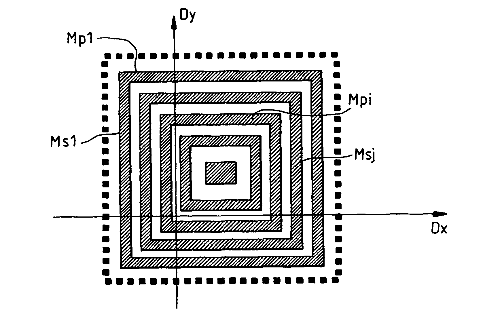
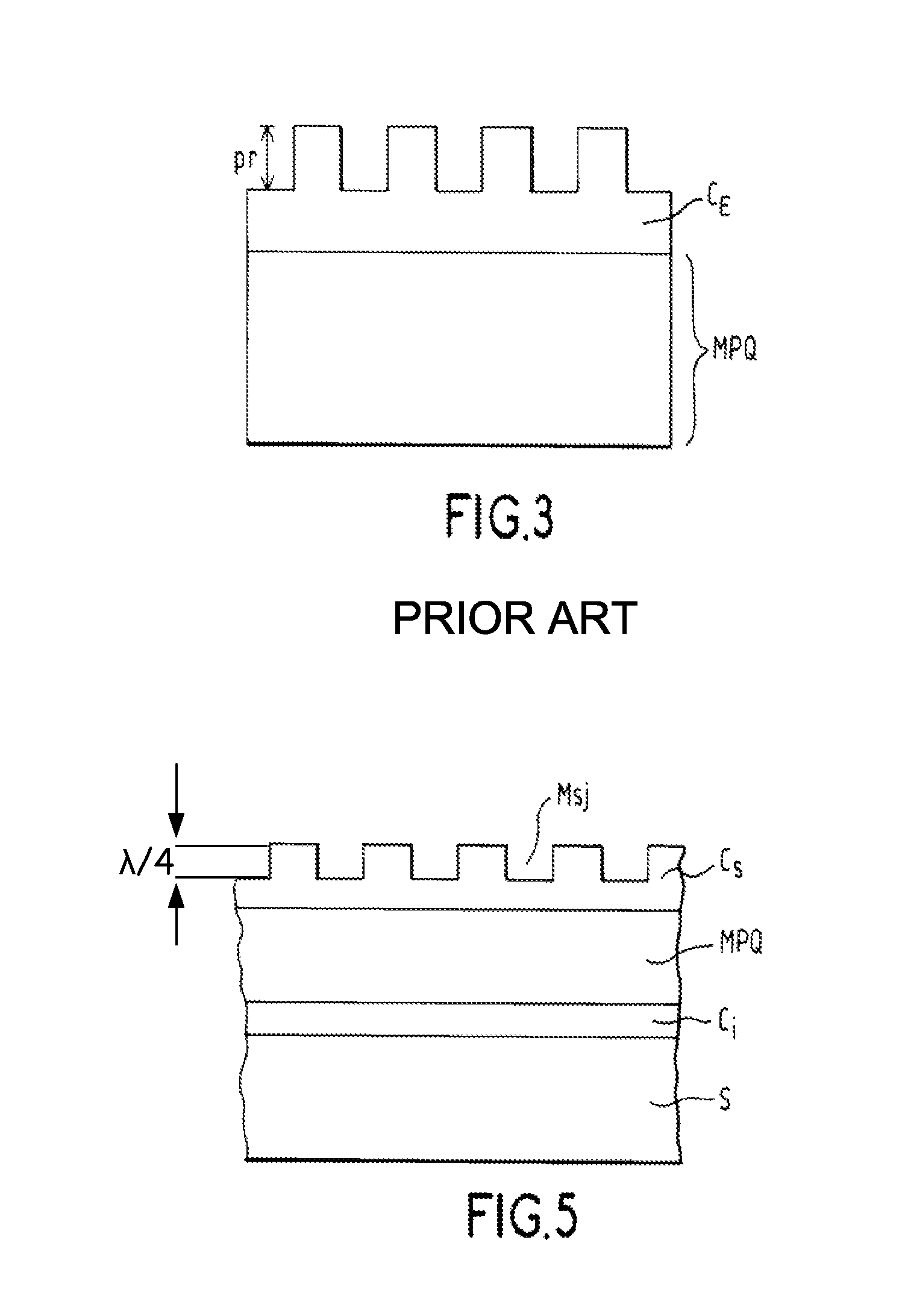
[0050]The lamellar features are produced within this upper contact layer.

[0051]To obtain the desired diffracting effects at an operating wavelength around 9 microns, the etch depths are 0.7 microns and the spacing of the featu...


PUM


Abstract

The invention relates to a detector comprising a multiple quantum well structure operating on interband or intersubband transitions by absorption of radiation having a wavelength λ having a polarization comprising a component perpendicular to the plane of the multiple quantum well structure, and comprising optical coupling means for coupling said radiation, wherein the coupling means comprise a set of first diffractive lamellar features that are distributed along at least a first direction and a set of second diffractive lamellar features that are distributed along at least a second direction, said first and second directions being mutually perpendicular and lying in a plane parallel to the plane of the multiple quantum well structure.

Description

FIELD OF THE INVENTION[0001]The field of the invention is that of electromagnetic wave detectors made of semiconductor material and especially one having a multiple quantum well structure, particularly one suitable for the infrared range.BACKGROUND OF THE INVENTION[0002]The rapid advances made in epitaxial growth on GaAs-type substrates has led to the development of a new class of electromagnetic wave detectors using the absorption of radiation around a wavelength λ corresponding to the electron transition between various energy levels within one and the same band or between the valence band and the conduction band. The diagram shown in FIG. 1 illustrates this type of transition.[0003]The recent evolution in performance of this type of component is due in particular to the relatively easy production of semiconductor heterojunction multilayers in the standard system by MBE (molecular beam epitaxy), that is to say the GaAs / Ga(1-x)AlxAs. By adjusting the growth parameters, the thicknes...

Claims


Application Information

Patent Timeline
Patent Type & Authority Patents(United States)
IPC IPC(8): H01L31/00H01L31/0232H01L31/0352
CPCB82Y20/00H01L31/035236H01L31/0232H01L31/02327
Inventor BOIS, PHILIPPECOSTARD, ERICDE ROSSI, ALFREDONEDELCU, ALEXANDRU
Owner THALES SA
Why Eureka
Try Eureka