Magnetic memory device using domain structure and multi-state of ferromagnetic material

a memory device and multi-domain technology, applied in the field of magnetic memory devices, can solve the problems of high voltage, complicated structure, and long time required to operate the dram back to the initial state, and achieve the effects of shortening the manufacturing process, reducing thickness, and increasing process efficiency

Active Publication Date: 2010-06-22
KOREA UNIV IND & ACADEMIC CALLABORATION FOUND +1
View PDF11 Cites 9 Cited by
  • Summary
  • Abstract
  • Description
  • Claims
  • Application Information

AI Technical Summary

Benefits of technology

[0013]Therefore, the present invention has been made in view of the above problems, and it is an object of the present invention to provide a magnetic memory device using a ferromagnetic materials (FM) having a stable multi-domain state, which has a reduced thickness and shortens a manufacturing process so as to increase an efficiency in the process.
[0014]It is another object of the present invention to provide a magnetic memory device using the stable single or multi-domain state of ferromagnetic materials (FM), which stores data of 4 states or more in one cell so as to increase a storage capacity and a processing speed of the device.

Problems solved by technology

DRAMs, which are most widely used now, are volatile memories that lose all stored data when the power is shut off, and thus require a long time to operate the DRAMs back to in an initial state.
The Fe RAMs are in a commercially usable state, but require a high voltage in an initial state and have a complicated structure.
However, the conventional MRAM device has a complicated structure due to the multiple magnetic layers forming spin valves and layers firming word lines and read lines, thus having problems, such as a difficulty in a manufacturing process and deterioration in productivity.

Method used


Image

  • Magnetic memory device using domain structure and multi-state of ferromagnetic material
  • Magnetic memory device using domain structure and multi-state of ferromagnetic material
  • Magnetic memory device using domain structure and multi-state of ferromagnetic material

Examples


embodiment

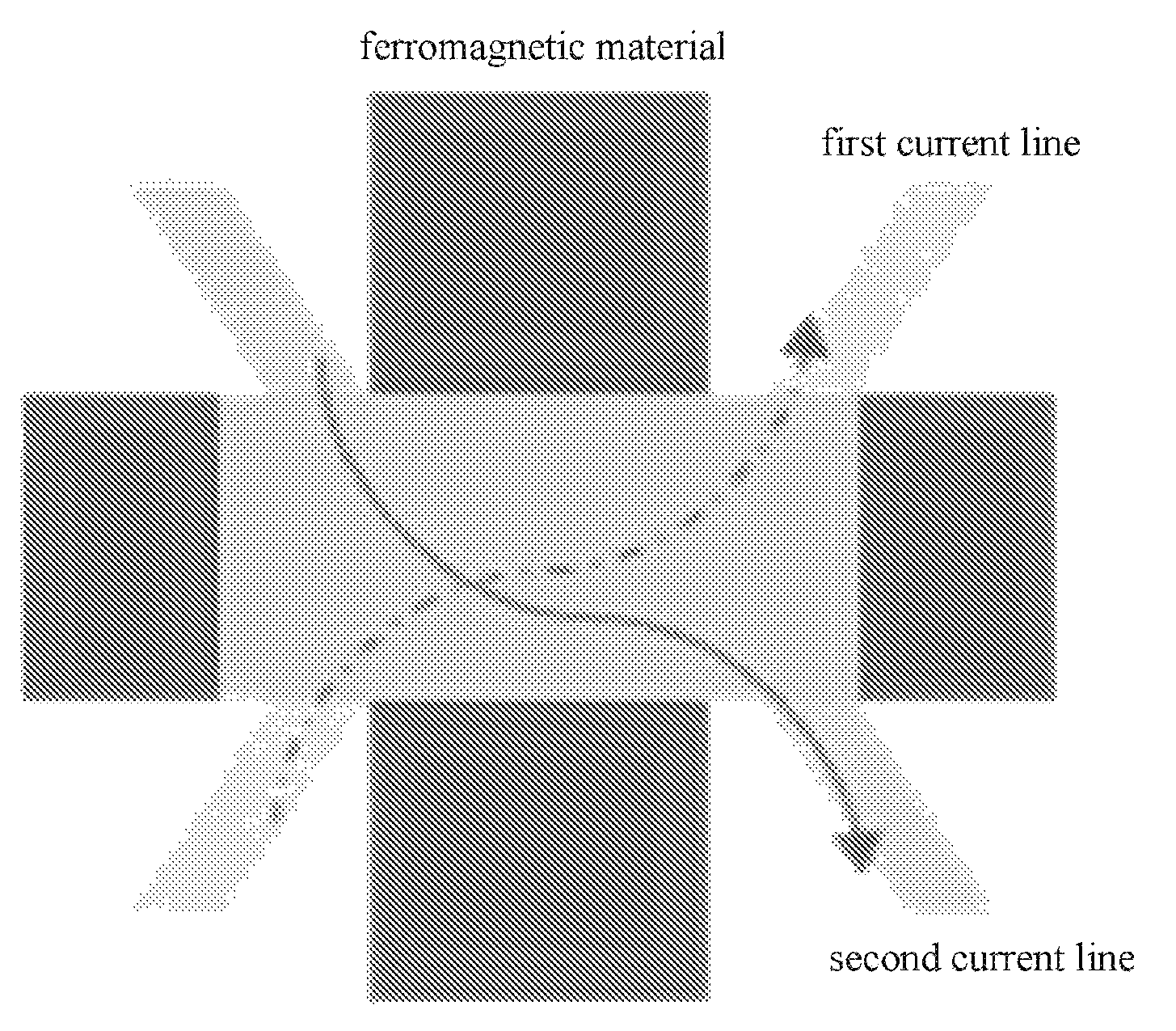
[0071]An external magnetic field for forming a single domain state or a multi-domain state is substituted by an induced magnetic field, obtained by forming current lines on a ferromagnetic semiconductor layer. FIG. 7 is a schematic view illustrating a structure for forming an induced magnetic field in accordance with the present invention, and FIG. 8 is a schematic view illustrating the formation of an induced magnetic field of a magnetic memory device in accordance with a preferred embodiment of the present invention.

[0072]With reference to FIGS. 7 and 8, current lines, distinguished from each other by an insulating layer, are formed in cells for storing data, and current in a pulse mode flows into the cells, in which the current lines cross each other, thereby forming an induced magnetic field and thus allowing data to be recorded in the cells.

[0073]That is, when the current is adjusted to the pulse mode, the induced magnetic field is formed around the current lines and a planar h...


PUM


Abstract

Disclosed is a memory device using a multi-domain state of a semiconductor material, and more particularly to a magnetic memory device, in which a ferromagnetic layer for recording magnetic data serves as a sensing layer so as to have a simple structure, shorten a manufacturing process, and reduce the unit cost of production. The planar hall effect or magneto-resistance is used to measure multi-domain states so as to read data stored in a multi-level state.

Description

BACKGROUND OF THE INVENTION[0001]1. Field of the Invention[0002]The present invention relates to a memory device using a multi-domain states of a ferromagnetic material, and more particularly to a magnetic memory device, in which a ferromagnetic layer for recording magnetic data serves as a sensing layer so as to have a simple structure, shorten a manufacturing process, and reduce the unit cost of production. The planar hall effect or magneto-resistance is used to measure multi-domain states so as to read data stored in a multi-level state.[0003]The present invention relates generally to a memory device designed for memory or data storage. It also is related generally to electronic device which uses single or multi-domain states of ferromagnetic material for data storage. Particularly, this magnetic memory device is composed of thin ferromagnetic film which acts as recording layer as well as sensing layer, resulting in simple structure, shortened manufacturing process, and reduced c...

Claims


Application Information

Patent Timeline
Patent Type & Authority Patents(United States)
IPC IPC(8): G11C11/18
CPCG11C11/18G11C11/5607H01L43/08H01L43/06H01L27/222H10B61/00H10N52/00H10N50/10H01L27/105
Inventor LEE, SANG-HOONSHIN, DONG-YUN
Owner KOREA UNIV IND & ACADEMIC CALLABORATION FOUND
Why Eureka
Try Eureka