Method of manufacturing a semiconductor device and the semiconductor device

a manufacturing method and semiconductor technology, applied in the direction of semiconductor devices, basic electric elements, electrical appliances, etc., can solve the problems of increasing the possibility of following inconvenience, voids tending to occur inside the trench, and the embedding characteristic deterioration, so as to achieve less failure, high degree of integration, and high degree of integration

Active Publication Date: 2010-06-29
MICRON TECH INC
View PDF16 Cites 9 Cited by
  • Summary
  • Abstract
  • Description
  • Claims
  • Application Information

AI Technical Summary

Benefits of technology

[0020]Halogen elements are of the seventeenth group of the periodic system. Chlorine (Cl2) and bromine (Br2) are gases at room temperature, and can be used as an oxidizing species (reactive gas) rich in reactivity. It is considered that the halogen element is not directly involved in oxidation as an oxidizing species, but functions as a catalyst, and acts to promote bonding of oxygen and silicon. Further, for the reasons that the concentrations of oxygen and halogen element are high near the shoulder portion of the trench, and that oxygen molecules and halogen molecules are able to move freely near the shoulder portion, in the shoulder portion of the trench is formed a thick oxide film that can be distinguished from typical isotropic oxidation. Among factors having an effect on the oxidizing rate of the halogen oxidation method are crystal face orientation, and the position and shape of a portion to be oxidized. Particularly, the oxidation method using DCE (dichloroethylene) exhibits remarkable anisotropy, and therefore, is suitable for efficient formation of an anisotropic oxide film.
[0044]Furthermore, in another preferred aspect of the semiconductor device of the invention, the semiconductor device is Flash Memory. The Flash Memory has a high degree of integration and less failure.

Problems solved by technology

In other words, when an upper end portion (shoulder portion) of a trench formed in a semiconductor substrate is not rounded and remains a shape with an acute angle, the possibility of causing following inconvenience increases.
The embedding characteristic deteriorates when an insulating layer is embedded in the trench, and a void tends to occur inside the trench (particularly, near the surface of the trench).
Further, the leak current tends to occur in the upper end portion of the trench.
Further, such inconvenience tends to occur that an insulating layer embedded in the trench rises in the upper end portion of the trench, thereby loses the flatness, and has an adverse effect on a conductive layer provided on the insulating layer.

Method used


Image

  • Method of manufacturing a semiconductor device and the semiconductor device
  • Method of manufacturing a semiconductor device and the semiconductor device
  • Method of manufacturing a semiconductor device and the semiconductor device

Examples


embodiment 1

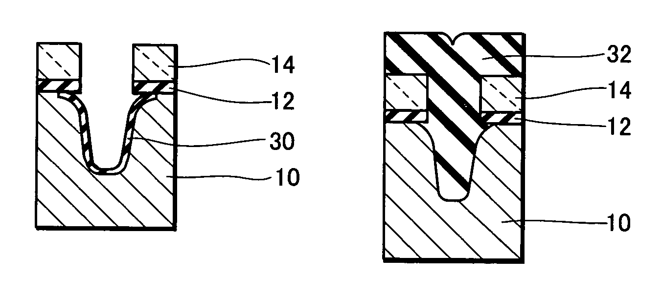
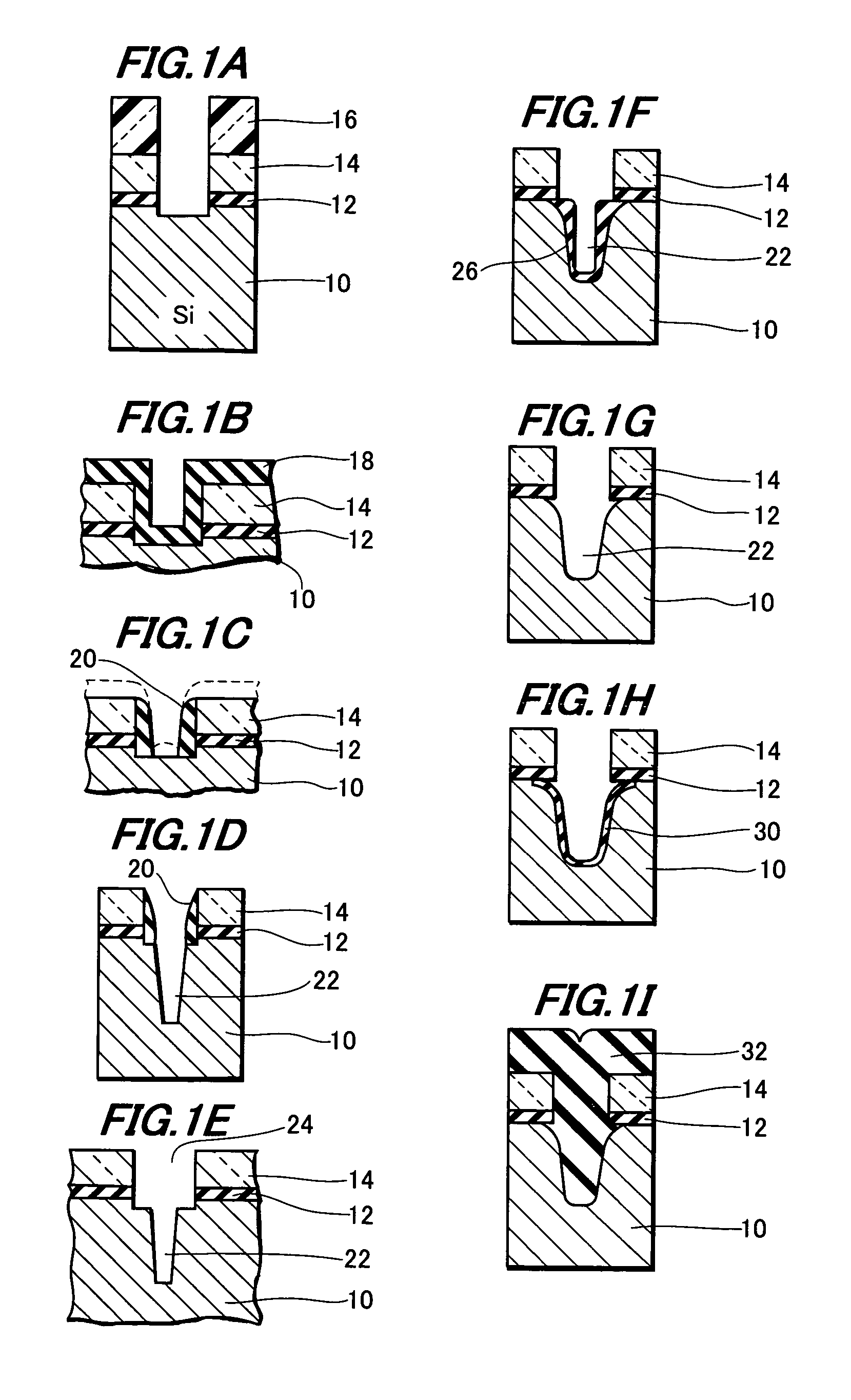
[0077]FIGS. 1A to 1I are cross-sectional views of main part of a device for each primary step showing from an initial step to a deposit step of an oxide film to embed in a trench in an example of a method of forming a trench of the invention.

[0078]Primary features of the manufacturing process as shown in FIG. 1 are that a side wall 20 is formed in a step of forming a trench processing mask (FIG. 1C), anisotropic oxidation is carried out after removing the side wall 20 and broadening an opening (FIGS. 1E and 1F), and that the area of the opening is intentionally increased by removing the anisotropic oxide film and preferentially backing off an upper end portion (shoulder portion) of a trench, while rounding a corner portion sufficiently (FIG. 1G). The aforementioned features will specifically be described below.

[0079]First, as shown in FIG. 1A, a silicon oxide film 12 with a thickness ranging from about 10 to 20 nm is formed on a semiconductor substrate (p-type silicon substrate) 10 ...

embodiment 2

[0163]This Example describes an example of forming an isotropic oxide film (SiO2) and silicon nitride film (SiN) in the trench.

[0164]It is a feature of this Example that after an isotropic oxide film is formed in the trench, a thin silicon nitride film 31 is formed on the surface of the isotropic oxide film, and embedding of the trench is then performed.

[0165]The silicon nitride film acts to prevent the occurrence of a situation that the oxide film on the surface of the trench is supplied with oxygen from the embedded oxide film (TEOS oxide film) and grows (expands) unnecessarily in performing heat treatment in subsequent steps.

[0166]When the oxide film on the surface of the trench expands even slightly, the width of the trench increases, and such fears arise that the stress between the silicon substrate and oxide film increases to increase the interface state density, and that the leak current increases. Therefore, the nitride film is provided as a buffer between the embedded oxide...

embodiment 3

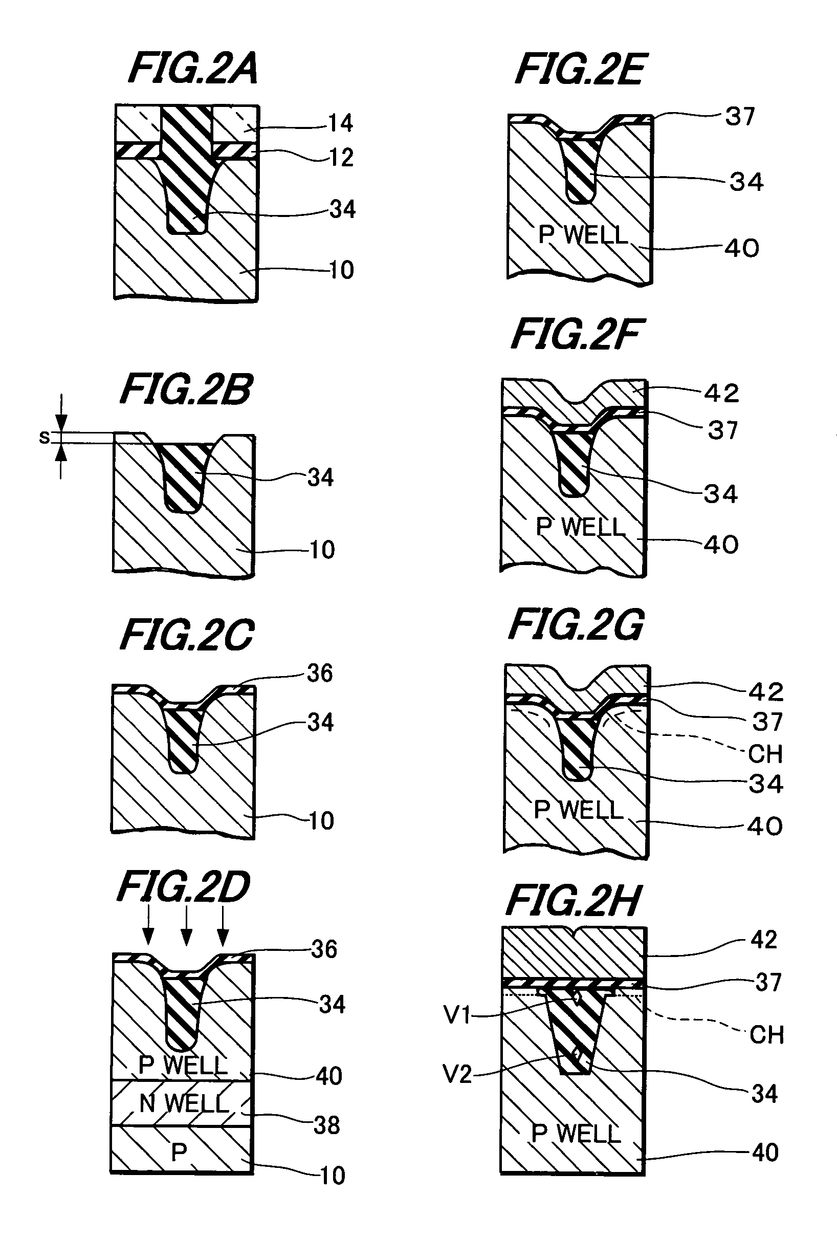
[0178]With reference to FIGS. 6 to 10, this Example describes the feature (such that the channel conductance can be increased in the MOS transistor) of a semiconductor device formed by using the method of forming a trench and the method of manufacturing a semiconductor device of the present invention, and specific examples of the semiconductor device.

[0179]FIG. 6 is a plan view of main part of a semiconductor device with integrated insulating gate type field-effect transistors (MOS transistors) manufactured by the method of forming a trench and the method of manufacturing a semiconductor device of the invention. In addition, in the FIG. 6, the same portions as in the drawings described above are assigned the same reference numerals.

[0180]In FIG. 6, two n-MOS transistors are formed in a region surrounded by the oxide film 34 (STI) embedded in the trench. In the figure, reference numerals 50a, 50b and 50c denote an n+-type diffusion region (region to be a source / drain), and reference ...


PUM


Abstract

The present invention provides a method of manufacturing a trench with a rounded corner portion and a broadened opening. Anisotropic oxidation is carried out using a halogen oxidation method using dichloroethylene (DCE) to form an anisotropic oxide film such that the film thickness in a shoulder portion of the trench is thick and gradually decreases nearer the bottom, the anisotropic oxide film is removed, and the shoulder portion of the trench is preferentially backed off, thereby rounding the shoulder portion sufficiently to broaden the opening. Then, an insulating member is embedded in the trench. The rounded portion of the shoulder portion of the trench and vicinity thereof is used as a channel of a MOS transistor.

Description

BACKGROUND OF THE INVENTION[0001]In recent years, as an element isolation structure in an LSI device, an STI (Shallow Trench Isolation) structure has been adopted that enables dimensions of an element isolation region to be controlled with high accuracy, as a substitute for a LOCOS structure. The STI structure is an element isolation structure that is formed by forming a shallow trench with an almost perpendicular side wall in a semiconductor substrate and embedding an insulating layer in the trench and that is suitable for high-integration LSI.[0002]The importance of rounding an upper corner portion in forming a trench has conventionally been pointed out (for example, JP 2000-299374).[0003]In other words, when an upper end portion (shoulder portion) of a trench formed in a semiconductor substrate is not rounded and remains a shape with an acute angle, the possibility of causing following inconvenience increases.[0004]Concentration of an electric field tends to occur. The embedding ...

Claims


Application Information

Patent Timeline
Patent Type & Authority Patents(United States)
IPC IPC(8): H01L21/76
CPCH01L21/76235H01L29/785
Inventor YAMAMOTO, HIROHISA
Owner MICRON TECH INC
Why Eureka
Try Eureka