Semiconductor device

a technology of semiconductor devices and semiconductors, applied in the direction of semiconductor devices, semiconductor/solid-state device details, electrical devices, etc., can solve the problems of uniform heat generation inside the device, greater amount of power consumed, and heat generated in the operating layer, so as to achieve significant heat uniformization effect and save spa

Active Publication Date: 2010-07-20
PANASONIC CORP
View PDF14 Cites 76 Cited by
  • Summary
  • Abstract
  • Description
  • Claims
  • Application Information

AI Technical Summary

Benefits of technology

[0011]An object of the present invention is to solve the conventional problems described above and to provide a semiconductor device using a group-III nitride semiconductor, saving space, and having a significant heat uniformization effect.
[0013]Moreover, preferably, a second semiconductor device according to the present invention includes: a first group-III nitride semiconductor layer formed on a substrate; a second group-III nitride semiconductor layer made of a single layer or two or more layers, formed on the first group-III nitride semiconductor layer, and acting as a barrier layer; and a first source electrode, a drain electrode, and a gate electrode formed on the second group-III nitride semiconductor layer, the gate electrode controlling a current flowing between the source and drain electrodes, the device further includes a via hole penetrating the operating layer, the barrier layer, and the substrate, and as a surface passivation film, a heat radiation film with high thermal conductivity covers the entire surface other than a bonding pad including the inside of the via hole. This is because with such a structure, the via hole can effectively uniformize heat staying ununiformly inside the semiconductor.
[0015]Preferably, the first or second semiconductor device uses, as the heat radiation film, diamond, diamond-like carbon (DLC), carbon, or a stacked film including at least two of the listed materials. This is because diamond, DLC, and carbon have insulative properties and concurrently a thermal conductivity equal to or higher than metal, so that they can effectively uniformize heat staying ununiformly inside the semiconductor.
[0016]Preferably, in the first or second semiconductor device, an insulating layer different from the heat radiation film is formed between the heat radiation film and the semiconductor layer. This is because a material with high adhesion can be provided to enhance the adhesion of the heat radiation film.

Problems solved by technology

This is because the higher voltage and the larger current an application has, the greater amount of power is consumed in and the greater amount of heat is generated from the semiconductor device.
In particular, for HFETs of multifinger structures commonly employed as power semiconductor devices handling large electric power, because of their structures, heat generated in the operating layer stays ununiformly inside the device.
The use of such a heat radiating component, however, requires a space enough to accommodate the component, which goes against the trend toward savings in the device space.

Method used


Image

  • Semiconductor device
  • Semiconductor device
  • Semiconductor device

Examples


first embodiment

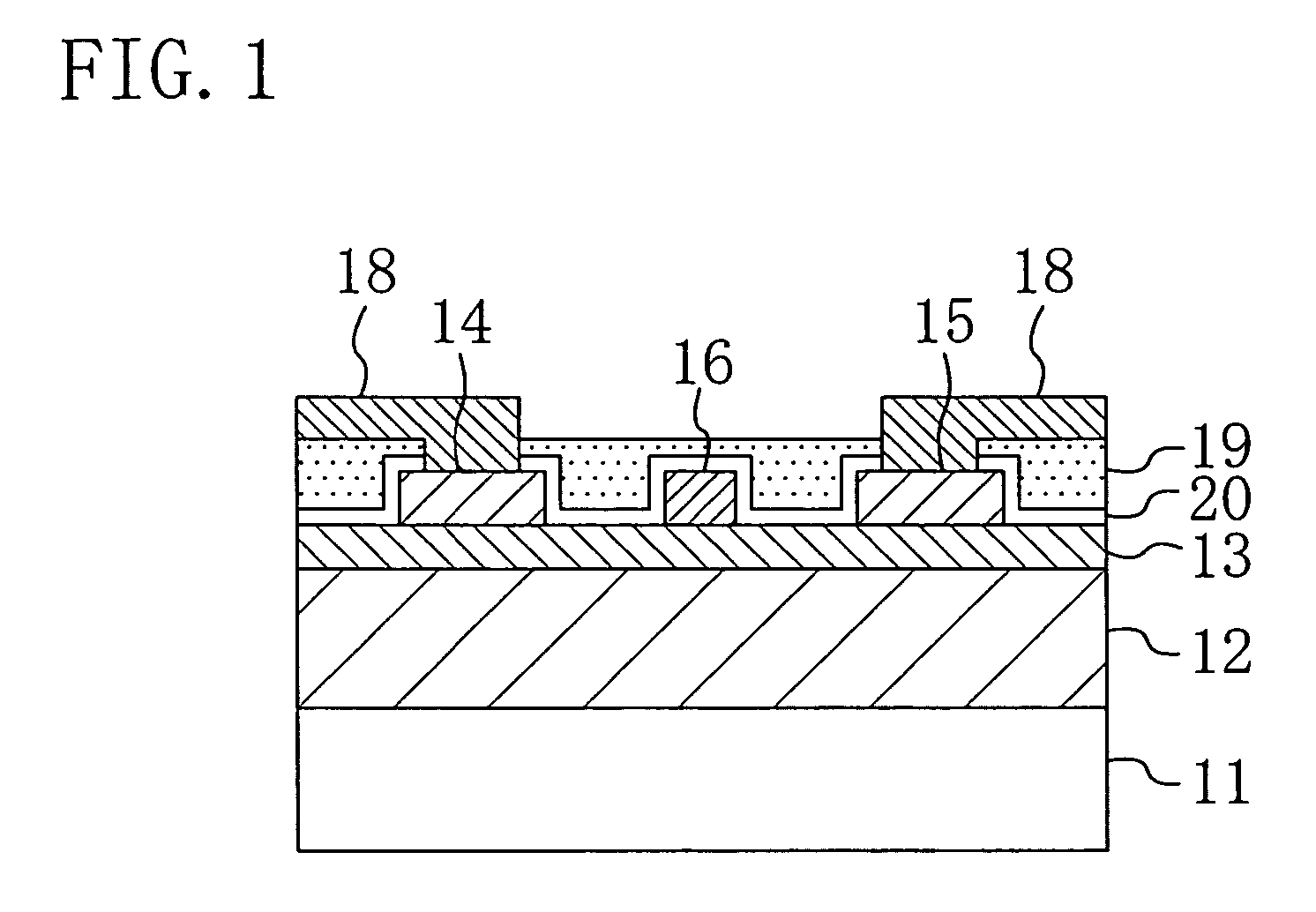
[0023]A semiconductor device according to a first embodiment of the present invention will be described with reference to FIG. 1.

[0024]FIG. 1 schematically shows a cross section of the semiconductor device according to the first embodiment.

[0025]Referring to FIG. 1, a barrier layer 13 of AlxGa(1-x)N (0≦x≦1) is stacked on an operating layer 12 of GaN formed on a substrate 11, and the operating layer 12 and the barrier layer 13 form a heterojunction interface. A source electrode 14 and a drain electrode 15 are formed away from each other, and a gate electrode 16 is formed between the source electrode 14 and the drain electrode 15. Bonding pad 18 is also provided connected to the source electrode 14 and / or the drain electrode 15. The surfaces of these electrodes and the barrier layer 13 are coated with an insulating film 20 made of a carbon compound (for example, titanium carbon (TiC) or aluminum carbon (AlC)) with high adhesion. The top of the insulating film 20 is coated with a diamo...

second embodiment

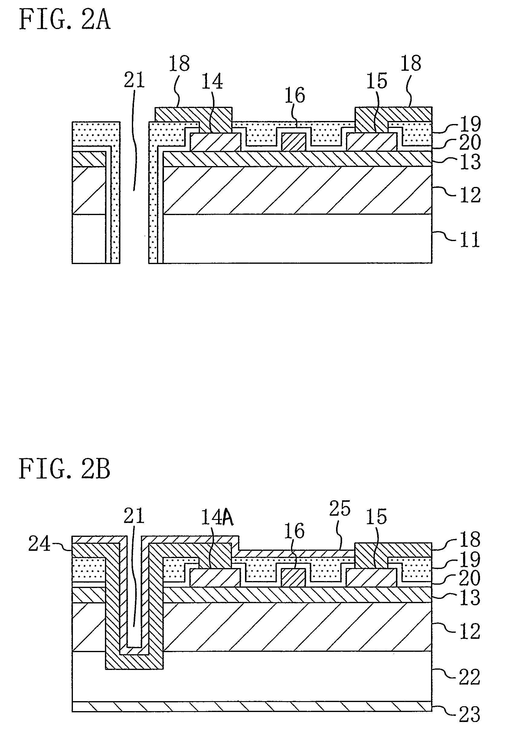
[0026]A semiconductor device according to a second embodiment of the present invention will be described with reference to FIG. 2.

[0027]FIG. 2A schematically shows a cross section of the semiconductor device according to the second embodiment.

[0028]Referring to FIG. 2A, a barrier layer 13 of AlxGa(1-x)N (0≦x≦1) is stacked on an operating layer 12 of GaN formed on a substrate 11, and the operating layer 12 and the barrier layer 13 form a heterojunction interface. A first source electrode 14A and a drain electrode 15 are formed away from each other, and a gate electrode 16 is formed between the first source electrode 14A and the drain electrode 15. The surfaces of these electrodes and the barrier layer 13 are coated with an insulating film 20 made of a carbon compound (for example, titanium carbon (TiC) or aluminum carbon (AlC)) with high adhesion. The top of the insulating film 20 is coated with a diamond film 19 having high thermal conductivity and excellent heat radiation property ...

third embodiment

[0031]A semiconductor device according to a third embodiment of the present invention will be described with reference to FIG. 3.

[0032]FIG. 3 schematically shows a cross section of the semiconductor device according to the third embodiment.

[0033]Referring to FIG. 3, a barrier layer 13 of AlxGa(1-x)N (0≦x≦1) is stacked on an operating layer 12 of GaN formed on a substrate 11, and the operating layer 12 and the barrier layer 13 form a heterojunction interface. On the both sides of a source electrode 14, a pair of drain electrodes 15 are formed away from each other, and a pair of gate electrodes 16 are formed between the source electrode 14 and the pair of drain electrodes 15, respectively. The surfaces of these electrodes and the barrier layer 13 are coated with an insulating film 20 made of a carbon compound (for example, titanium carbon (TiC) or aluminum carbon (AlC)) with high adhesion. The top of the insulating film 20 is coated with a diamond film 19 having high thermal conductiv...


PUM


Abstract

A semiconductor device includes: a first group-III nitride semiconductor layer formed on a substrate; a second group-III nitride semiconductor layer made of a single layer or two or more layers, formed on the first group-III nitride semiconductor layer, and acting as a barrier layer; a source electrode, a drain electrode, and a gate electrode formed on the second group-III nitride semiconductor layer, the gate electrode controlling a current flowing between the source and drain electrodes; and a heat radiation film with high thermal conductivity which covers, as a surface passivation film, the entire surface other than a bonding pad.

Description

CROSS-REFERENCE TO RELATED APPLICATIONS[0001]This application claims priority under 35 U.S.C. §119 on Patent Application No. 2005-347988 filed in Japan on Dec. 1, 2005, the entire contents of which are hereby incorporated by reference.BACKGROUND OF THE INVENTION[0002](a) Fields of the Invention[0003]The present invention relates to semiconductor devices employing a group-III nitride semiconductor. In particular, the present invention relates to power semiconductor devices of a group-III nitride semiconductor handling large electric power and having excellent heat radiation.[0004](b) Description of Related Art[0005]Group-III nitride semiconductors refer to compound semiconductors which are made of a compound of nitrogen (N) and aluminum (Al), boron (B), gallium (Ga), or indium (In) represented by a general formula BwAlxGayInzN (w+x+y+z=1; 0≦w,x,y,z≦1).[0006]The group-III nitride semiconductors have advantages such as wide band gap and high breakdown voltage associated with this gap, ...

Claims


Application Information

Patent Timeline
Patent Type & Authority Patents(United States)
IPC IPC(8): H01L31/0256
CPCH01L23/3732H01L29/66462H01L29/7787H01L29/2003H01L2924/0002H01L2924/00
Inventor UENO, HIROAKIYANAGIHARA, MANABUUEMOTO, YASUHIROTANAKA, TSUYOSHI
Owner PANASONIC CORP
Why Eureka
Try Eureka