Piezo-diode cantilever MEMS

a diode and diode technology, applied in the direction of microstructural devices, acceleration measurement using interia forces, instruments, etc., can solve the problems of changing electrical current and strain across a large surface area to create current changes, and achieve enhanced mechanical strain, enhanced chemical vapor deposition, and reduced mems

Inactive Publication Date: 2010-07-27
SHARP KK
View PDF9 Cites 19 Cited by
  • Summary
  • Abstract
  • Description
  • Claims
  • Application Information

AI Technical Summary

Benefits of technology

[0011]Sensitivity and signal-to-noise ratio are two important parameters for MEMS sensors. The present invention piezo-diode cantilever MEMS sensor converts mechanical energy (surface stress) induced on a molecule-solid interface to electrical energy. Reducing the MEMS structure thickness effectively enhances the mechanical strain induced by surface stress. In one aspect, the present invention uses a plasma enhanced chemical vapor deposition (PECVD) method to control the MEMS structure thickness, and uses a pre-deposited sacrificial film to support the MEMS structure fabrication and define the air gap between a MEMS structure and the substrate. The sacrificial film is removed to free the MEMS structure after all fabrication steps are completed. While the prior art uses either a SOI substrate to control MEMS structure thickness or a high temperature LPCVD process, the present invention sensor can be fabricated on any substrate, using conventional mass production processes for low cost consumer applications, due to the low process temperature of the PECVD processes.

Problems solved by technology

If the P-I-N diode is fabricated on an amorphous film, the mechanical strain change on the amorphous film affects its current transport mechanism in the diode, resulting in a change in electrical current.
However, due to the high density of defects in amorphous silicon, the strain across a large surface area is required to create current changes large enough to easily detect.

Method used


Image

  • Piezo-diode cantilever MEMS
  • Piezo-diode cantilever MEMS
  • Piezo-diode cantilever MEMS

Examples


Embodiment Construction

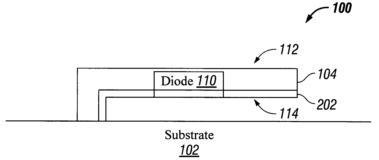
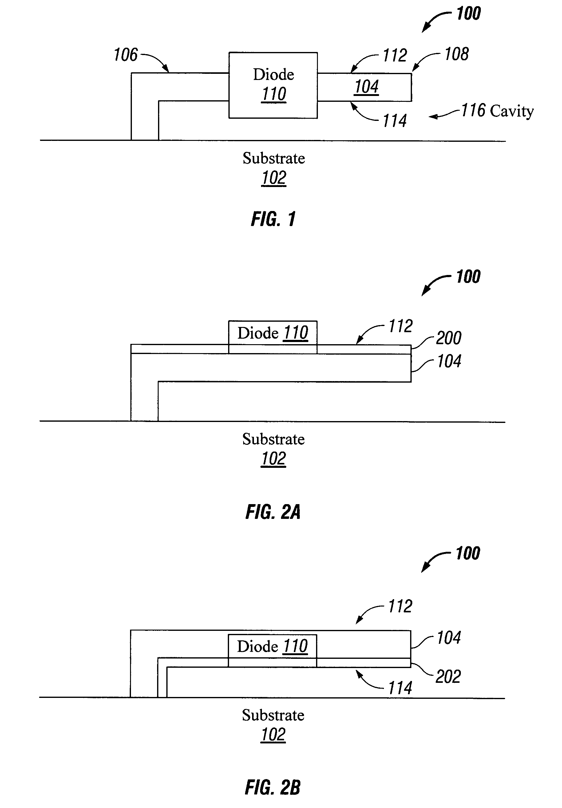
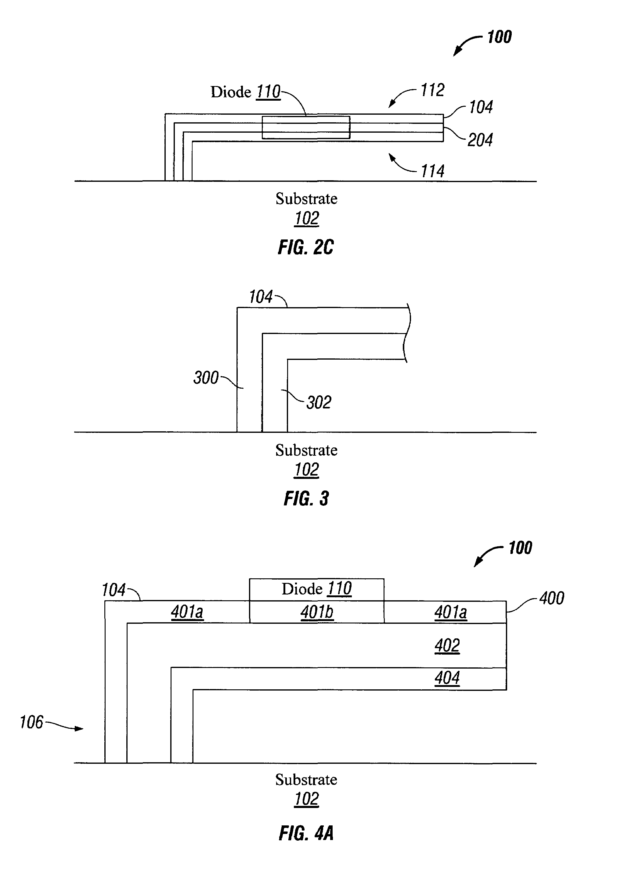
[0025]FIG. 1 is a partial cross-sectional view of a piezo thin-film diode (piezo-diode) cantilever microelectromechanical system (MEMS). The piezo-diode cantilever 100 comprises a substrate 102. Some possible substrate materials include glass, polymer, quartz, metal foil, Si, Si-containing materials, sapphire, ceramic, and compound semiconductor materials, such as Si-germanium for example. A multi-layered film cantilever beam 104 has a distal end 106 anchored to the substrate 102, and a proximal end 108. A diode 110 is embedded in the cantilever beam 104 and shares a film layer in common with the cantilever beam 104. The cantilever beam 104 has a top surface 112 and a bottom surface 114. A cavity 116 is formed between the cantilever beam proximal end 108 and the substrate 102.

[0026]The cantilever body can be a rectangular as shown, or shaped (e.g., as a triangle, circle, or oval), with one or multiple points for anchoring to the substrate. The cantilever beam 104 and diode 110 film ...


PUM

PropertyMeasurementUnit
temperatureaaaaaaaaaa
thicknessaaaaaaaaaa
grain sizeaaaaaaaaaa

Abstract

A piezo thin-film diode (piezo-diode) cantilever microelectromechanical system (MEMS) and associated fabrication processes are provided. The method deposits thin-films overlying a substrate. The substrate can be made of glass, polymer, quartz, metal foil, Si, sapphire, ceramic, or compound semiconductor materials. Amorphous silicon (a-Si), polycrystalline Si (poly-Si), oxides, a-SiGe, poly-SiGe, metals, metal-containing compounds, nitrides, polymers, ceramic films, magnetic films, and compound semiconductor materials are some examples of thin-film materials. A cantilever beam is formed from the thin-films, and a diode is embedded with the cantilever beam. The diode is made from a thin-film shared in common with the cantilever beam. The shared thin-film may a film overlying a cantilever beam top surface, a thin-film overlying a cantilever beam bottom surface, or a thin-film embedded within the cantilever beam.

Description

BACKGROUND OF THE INVENTION[0001]1. Field of the Invention[0002]This invention generally relates to the fabrication of microelectromechanical systems (MEMS) and, more particularly, to a thin-film diode cantilever MEMS and related fabrication procedures.[0003]2. Description of the Related Art[0004]Active devices such as thin-film transistors (TFTs) and diodes are formed through deposition processes that create thin films of silicon (Si) and insulator material. While the resulting devices may not have the switching speed and drive capability of devices formed on single-crystal substrates, they can be fabricated cheaply with a relatively few number of process steps. Further, thin-film deposition processes permit active devices to be formed on alternate substrate materials, such as transparent glass substrates, for use in liquid crystal displays (LCDs). More specifically, the active devices may include a deposited amorphous Si (a-Si) layer. To improve the performance of the device, the ...

Claims


Application Information

Patent Timeline
Patent Type & Authority Patents(United States)
IPC IPC(8): H01L41/113
CPCB81B3/0021H01L29/868
Inventor ZHAN, CHANGQINGSCHUELE, PAUL J.CONLEY, JR., JOHN F.HARTZELL, JOHN W.
Owner SHARP KK
Why Eureka
Try Eureka