Silicon carbide semiconductor device and manufacturing method therefor

a technology of silicon carbide and semiconductors, applied in semiconductor devices, semiconductor/solid-state device details, electrical devices, etc., can solve the problem of suppressing growth rate, suppressing basal plane dislocation from the substrate to the epitaxial film, and preventing forward voltage deterioration

Active Publication Date: 2010-08-03
THE KANSAI ELECTRIC POWER CO +1
View PDF19 Cites 11 Cited by
  • Summary
  • Abstract
  • Description
  • Claims
  • Application Information

AI Technical Summary

Benefits of technology

[0017]According to the technology disclosed herein, since the first- and second-conductive-type silicon carbide semiconductor layers are formed as described above, semiconductor layers less liable to basal plane dislocation can be obtained. As a result, a pn junction diode which is less liable to forward voltage deterioration and long in service life can be obtained.
[0044]According to the technology disclosed herein, since the propagation of the basal plane dislocation in the semiconductor layers is suppressed, forward voltage deterioration can be prevented. That is, the forward voltage difference ΔVf representing forward voltage deterioration can be suppressed to 1.0 V or less, so that a high-reliability bipolar device can be made up. With the use of such a high-reliability bipolar device, power conversion equipment, such as inverters, which are reduced in loss, capable of long-term operation and high in reliability can be implemented.

Problems solved by technology

However, since the CVD process employs hydrogen as the carrier gas, separation of carbon (C) from the growth surface occurs during the growth, causing the growth rate to be suppressed.

Method used


Image

  • Silicon carbide semiconductor device and manufacturing method therefor
  • Silicon carbide semiconductor device and manufacturing method therefor
  • Silicon carbide semiconductor device and manufacturing method therefor

Examples


first embodiment

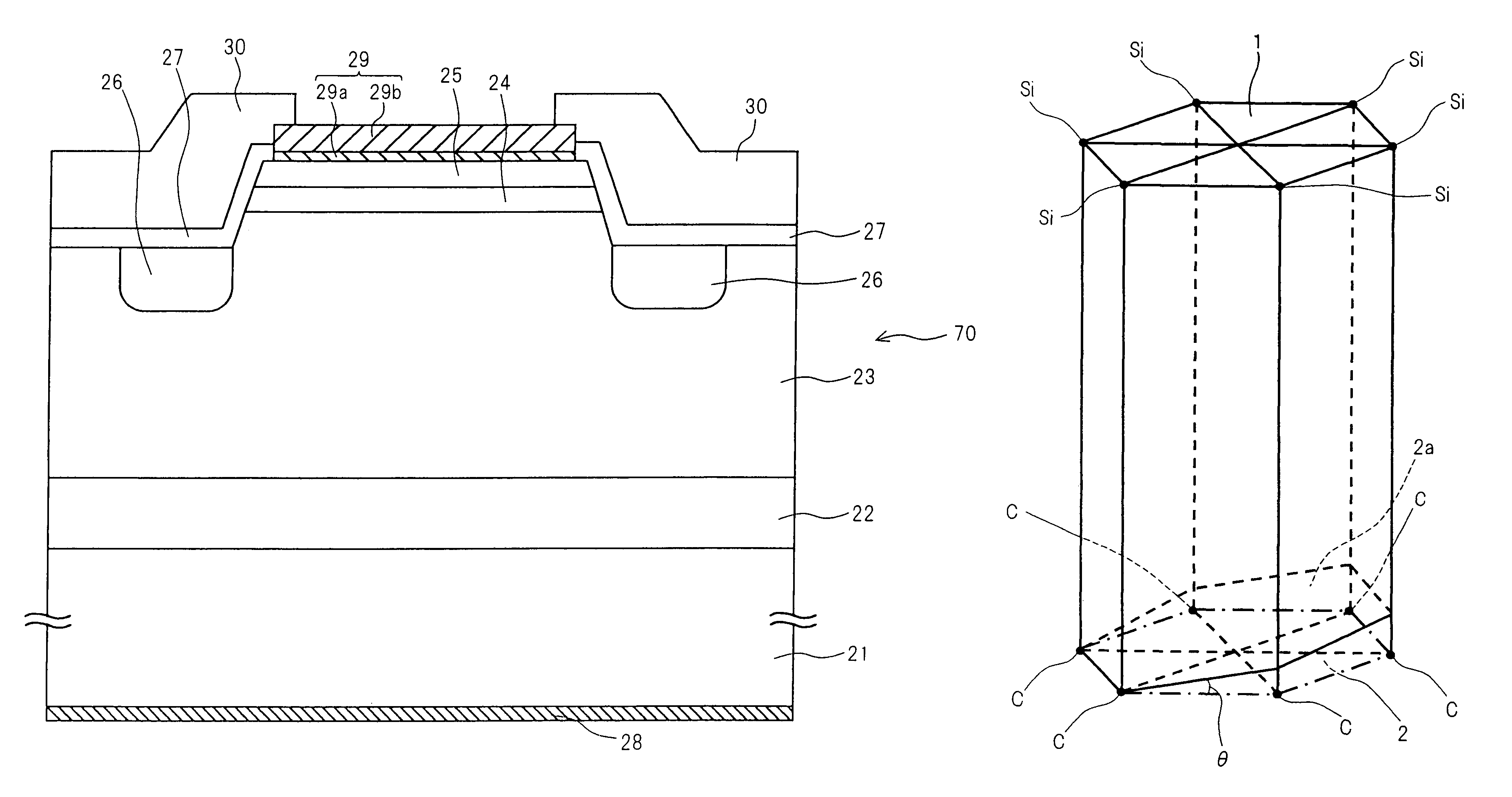
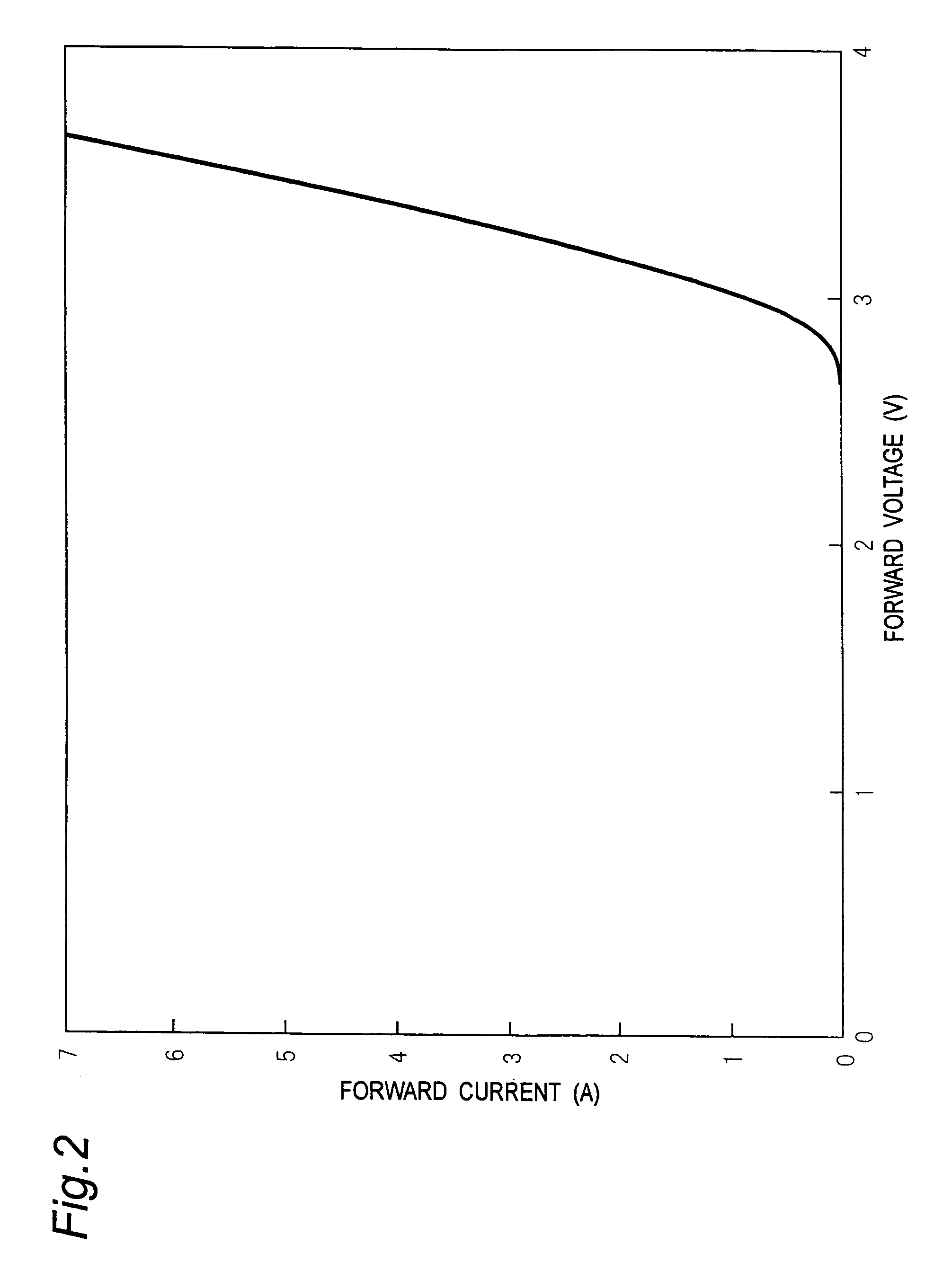
[0101]FIG. 1 is a sectional view of a pn (pin) junction diode which is a First Example Embodiment of a bipolar semiconductor device . In this Embodiment, semiconductor layers to be described below are formed on an p-p-type (first conductive type) 4H SiC substrate 21 whose surface orientation has an off-angle of 8 degrees from the (000-1) carbon surface. In the term “4H,” the character “H” means hexagonal crystal and the numeral “4” means a crystal structure whose atomic lamination is four-layer cyclic. The C surface of the substrate 21 is a surface 2a having an off-angle θ of 8 degrees from the (000-1) carbon surface 2 of SiC crystal of FIG. 6. The film growth rate for each layer is 15 μm / h, where the increasing rate of film thickness per hour (h) is faster than in the conventional counterpart. Then, as described in detail below, n-p-type (first conductive type) 4H-SiC layer and p-type (second conductive type) 4H-SiC layer are epitaxially grown one by one, by which an epitaxial pin ...

second embodiment

[0126]FIG. 4 is a sectional view of an npn bipolar transistor 50 which is a Second Example Embodiment of a bipolar semiconductor device. In this embodiment also, as shown in FIG. 6, an p-p-type 4H SiC substrate having a surface 2a whose surface orientation has an off-angle θ of 8 degrees from the (000-1) carbon surface 2 (hereinafter, referred to as C surface) is used. On this substrate, n-type 4H-SiC, p-type 4H-SiC and n-type 4H-SiC are successively epitaxially grown in this order with a film-thickness increasing rate per hour (h) of 15 μm / h, by which an npn bipolar transistor 50 was fabricated.

[0127]Also, n-type 4H-SiC having a surface 1a (hereinafter, referred to as Si surface) whose off-angle θ from the (0001) silicon surface 1 shown in FIG. 7 was 8 degrees was used as the substrate for an npn bipolar transistor for comparison use. On this substrate, individual layers were grown with a film-thickness increasing rate per hour (h) of 5 μm / h. The primary junction surface (a surface...

third embodiment

(Third Embodiment)

[0149]A Third Example Embodiment relates to an IGBT (Insulated Gate Bipolar Transistor) which is a bipolar semiconductor device . FIG. 5 is a sectional view of an IGBT 60 of this Embodiment. In this Embodiment, a substrate 61 (hereinafter, referred to as C surface substrate) using n-type 6H SiC whose surface orientation has an off-angle θ of 3.5 degrees from the (000-1) carbon surface 2 in FIG. 6 is prepared. On the substrate 61, three layers, i.e. a p-type 6H-SiC layer, an n-type 6H-SiC layer and a p-type 6H-SiC layer, are epitaxially grown in this order with a film-hickness increasing rate per hour (h) of 15 μm / h, by which an IGBT 60 is fabricated as is explained in detail below. The primary junction surface (a surface extending horizontally in the figure) of the p and n layers is the {0001} surface.

[0150]A comparative IGBT for comparison with the IGBT of this Embodiment is fabricated in the following way. A substrate (hereinafter, referred to as Si surface subst...


PUM

PropertyMeasurementUnit
off-angleaaaaaaaaaa
forward voltageaaaaaaaaaa
off-angleaaaaaaaaaa

Abstract

With a view to preventing increases in forward voltage due to a change with the lapse of time of a bipolar semiconductor device using a silicon carbide semiconductor, a buffer layer, a drift layer and other p-type and n-type semiconductor layers are formed on a growth surface, which is given by a surface of a crystal of a silicon carbide semiconductor having an off-angle θ of 8 degrees from a (000-1) carbon surface of the crystal, at a film growth rate having a film-thickness increasing rate per hour h of 10 μm / h, which is three times or more higher than conventional counterparts. The flow rate of silane and propane material gases and dopant gases is largely increased to enhance the film growth rate.

Description

[0001]This application is the U.S. national phase of international application PCT / JP2004 / 017888 filed 1 Dec. 2004, which designated the U.S. and claims benefit of JP 2003-405259 filed 3 Dec. 2003, the entire contents of each of which are hereby incorporated by reference.TECHNICAL FIELD[0002]The present invention relates to a silicon carbide bipolar semiconductor device suitable for control of large currents.BACKGROUND ART[0003]Wide-gap semiconductor materials including silicon carbide (SiC) have such excellent characteristics as their high dielectric breakdown field strengths, which are about ten times higher than that of silicon (Si), and thus have been drawing attention as materials suitable for high withstand voltage bipolar power semiconductor devices having high withstand reverse voltage characteristics.[0004]Bipolar semiconductor devices such as pin (Positive Intrinsic Negative) diodes, bipolar transistors, GTO (Gate Turn-Off Thyristor) and GCT (Gate-Commutated Thyristor), al...

Claims


Application Information

Patent Timeline
Patent Type & Authority Patents(United States)
IPC IPC(8): H01L29/15H01L31/0312H01L21/331H01L21/04H01L21/329H01L21/336H01L29/04H01L29/12H01L29/24H01L29/73H01L29/739H01L29/78H01L29/861
CPCH01L29/045H01L29/0619H01L29/1608H01L29/66068H01L29/73H01L29/7397H01L29/868H01L21/20
Inventor NAKAYAMA, KOJISUGAWARA, YOSHITAKAASANO, KATSUNORITSUCHIDA, HIDEKAZUKAMATA, ISAHOMIYANAGI, TOSHIYUKINAKAMURA, TOMONORI
Owner THE KANSAI ELECTRIC POWER CO
Why Eureka
Try Eureka