Electronic circuit device

a technology of electronic circuit and circuit device, applied in the direction of pulse technique, radio frequency controlled device, instruments, etc., can solve the problem of limitation of input signals, and achieve the effect of reducing electromagnetic waves, and preventing unnecessary electromagnetic waves

Inactive Publication Date: 2010-08-03
SEMICON ENERGY LAB CO LTD +1
View PDF126 Cites 11 Cited by
  • Summary
  • Abstract
  • Description
  • Claims
  • Application Information

AI Technical Summary

Benefits of technology

[0009]In order to solve the above-described problems, in the present invention, an electronic circuit substrate which configures an electronic circuit device is configured with a transparent substrate (hereinafter written as a substrate or a transparent substrate), a signal is inputted optically, an optical shutter and an optical sensor are provided and set over the transparent substrate, and a transmission and reception of a signal are performed using a light, whereby a occurrence of unnecessary electromagnetic waves is prevented. Further, more parallel processing is enabled by providing a number of optical sensors and optical shutters which receive light. In this way, the signal frequency is lowered and the electromagnetic waves can be reduced further.
[0010]An electronic circuit device of the present invention comprises a plurality of transparent substrates, and an optical sensor and an optical shutter are formed over the transparent substrate. An optical signal is inputted from an external to the electronic circuit device and the optical signal is directly irradiated on the optical sensor disposed over the transparent substrate, or the optical signal is transmitted through the transparent substrate and inputted into an optical sensor disposed over another substrate. The optical sensor converts the optical signal into an electronic signal, and a circuit disposed over the substrate is driven. A control signal controls the optical shutter, an input of light is carried out from the external to this optical shutter, and whether the light is transmitted through the optical shutter or the light is interrupted is determined, thereby taking out a signal. This control signal may be an output of the circuit over the substrate or a signal outputted from another circuit. In this way, an unnecessary occurrence of electromagnetic waves is prevented by performing the input and the output using the optical signal.

Problems solved by technology

Additionally, in the conventional electronic circuit units, substrates are connected to one another with wirings; there are limitations to input signals in parallel and the signal frequency must be set high.

Method used


Image

  • Electronic circuit device
  • Electronic circuit device
  • Electronic circuit device

Examples


embodiment 1

[0046]An optical sensor part will be described in detail. FIG. 4 shows a circuit diagram of an optical sensor part according to the present invention. In the present embodiment, the optical sensor is configured with a photodiode. An operation of the optical sensor part will be described below with reference to FIG. 4. First, a reset pulse is inputted into a reset transistor 405. Herein, since a TFT of P-channel polarity (hereinafter written as Pch) is used for this reset transistor, a signal is active-low. When the reset transistor 405 is turned ON, a cathode potential of a photodiode 401 is raised to the level of potential of an electric source. At this time, a storage capacitor of a capacitor 402 is also similarly raised to the level of potential of the electric source. This storage capacitor of the capacitor 402 may not be particularly mounted when a capacitance of the photodiode 401 is large. Next, a reset pulse becomes high, and the reset transistor 405 is turned OFF.

[0047]In t...

embodiment 2

[0052]In the present Embodiment, an optical shutter is formed by using liquid crystal. As is generally known, a liquid crystal panel is fabricated by injecting a crystal liquid material into the cell gap in width of several μm, a transmittance of a light is controlled by an applied voltage and the liquid crystal functions as an optical shutter. The entire surface of a substrate does not need the function of crystal liquid necessarily, however, since the fabrication of the substrate becomes easier when a crystal liquid is injected over the entire surface of the substrate, in the present Embodiment, a crystal liquid has been injected. Although the fabrication becomes complex, a configuration in which the liquid crystal is eliminated from a light input section is also capable of being employed. In such a case, only a portion where an optical shutter exists is surrounded with a sealing material, and a liquid crystal may be injected only into that portion.

[0053]FIG. 8 shows a circuit dia...

embodiment 3

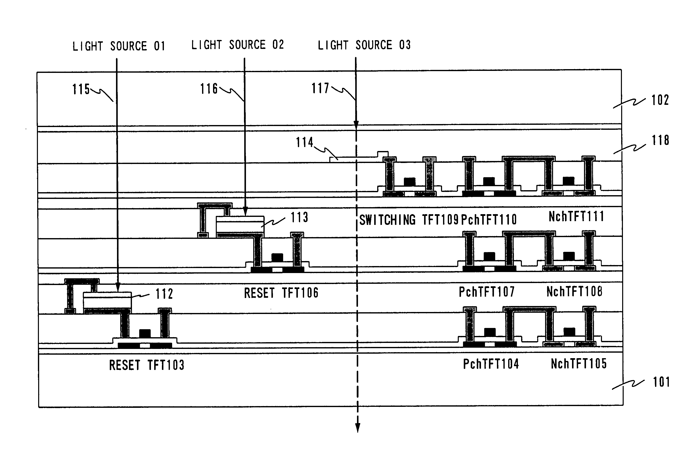
[0058]The steps according to the present invention will be described referring to a cross sectional view in FIG. 10. In FIG. 10, an optical sensor is configured with a TFT and an amorphous silicon photodiode, and an optical shutter is configured with a crystal liquid. In the present Embodiment, the TFT and the photodiode is formed by the following method. First, an overcoating film 1002 is formed over the glass substrate 1001. As for this film, an oxide film or a nitride film is formed by a Chemical Vapor Deposition method (hereinafter written as a CVD method). Next, an amorphous silicon is similarly formed into a film by a CVD method. The amorphous silicon film is crystallized by a laser annealing method, or a thermal annealing method. In this way, a polysilicon (p-Si) film can be formed. Next, TFT islands 1003, 1004 and 1005 are formed by patterning the polysilicon film. Then, a gate insulator 1006 is formed by a CVD method.

[0059]Then, as a method for forming a gate electrode, a m...


PUM

PropertyMeasurementUnit
frequencyaaaaaaaaaa
frequencyaaaaaaaaaa
transparentaaaaaaaaaa

Abstract

An object of the present invention is to provide an electronic circuit device capable of reducing the occurrence of electromagnetic waves associated with the propagation of a signal by utilizing light as a signal. The electronic circuit device has a transparent substrate (hereinafter written as a substrate) over which an optical sensor and an optical shutter and an electronic circuit composed of thin film transistors (TFTs) are formed. An optical signal is inputted from an external into the electronic circuit device, the optical signal is directly irradiated on the optical sensor over the substrate, and penetrates through the substrate, and inputted into an optical sensor over another substrate. The optical sensor converts the optical signal into an electronic signal, and the circuit over the substrate operates. A control signal controls the optical shutter, a light is inputted from the external into this optical shutter, and whether it is transmitted or it is interrupted is determined, whereby the signal is taken out.

Description

BACKGROUND OF THE INVENTION[0001]1. Field of the Invention[0002]The present invention relates to an electronic circuit device for light input, and particularly, relates to an electronic circuit device for light input, which is composed by forming a thin film transistor (hereinafter written as a TFT) over a transparent substrate such as substrate made of quartz, glass, plastic, or the like. Moreover, the present invention relates to an electronic device such as a computer or the like composed of the electronic circuit devices.[0003]2. Description of the Related Art[0004]At the present day, the informatization has been furthermore advanced with the improvement of electronic devices. It is expected that this tendency will be further promoted hereafter. In general, an electronic circuit device in wide spread use which configures an electronic device has the circuit over a printed circuit substrate (also called printed circuit board, hereinafter written as a printed circuit substrate). S...

Claims


Application Information

Patent Timeline
Patent Type & Authority Patents(United States)
IPC IPC(8): G02B6/12H04B10/00H01L27/14G02F1/01G02B6/43G02F1/13G02F3/00H01L21/336H01L27/144H01L29/786H01L31/10H04B10/11H04B10/40H04B10/50H04B10/60H04B10/67H04B10/80
CPCG02B6/43G02F3/00
Inventor IMAI, SHIGEKINAGAI, TOMOYUKIYAMAZAKI, SHUNPEIKOYAMA, JUN
Owner SEMICON ENERGY LAB CO LTD
Why Eureka
Try Eureka