Method for manufacturing semiconductor device

a manufacturing method and semiconductor technology, applied in the direction of semiconductor devices, basic electric elements, electrical appliances, etc., can solve the problems of difficult control of the thickness of the channel formation region and unstable step, and achieve the effect of restoring crystallinity, suppressing the increase in resistance of the source region or the drain region, and restoring crystallinity effectively

Inactive Publication Date: 2010-08-10
SEMICON ENERGY LAB CO LTD
View PDF5 Cites 5 Cited by
  • Summary
  • Abstract
  • Description
  • Claims
  • Application Information

AI Technical Summary

Benefits of technology

[0008]The present invention provides a technique for solving such problems. It is an object of the present invention to provide a method for manufacturing a highly responsive semiconductor device in which the subthreshold swing (S value) is small and reduction in on-current is suppressed without complicated steps.
[0012]In a semiconductor device of the present invention, the thickness of a source region or a drain region is larger than that of a channel formation region, which is advantageous in restoring the crystallinity in a heat treatment for thermal activation of an impurity element that is performed after addition of the impurity element by an ion doping method, an ion implantation method or the like. An increase in resistance of the source region or the drain region can be suppressed by restoring the crystallinity effectively. Further, since the thickness of the channel formation region is smaller than that of the source region or the drain region, the subthreshold swing (S value) can be decreased and reduction in on-current can be suppressed. Furthermore, since the semiconductor layer having a concavo-convex shape is formed by stacking semiconductor layers, the thickness can be easily controlled. Accordingly, a highly responsive semiconductor device in which the subthreshold swing (S value) is small and reduction in on-current is suppressed can be manufactured easily.

Problems solved by technology

However, in a conventional method, as described in Patent Document 1, there is a problem in that a step is unstable because a semiconductor layer needs to be etched as selected in order to form a channel formation region with a predetermined thickness, in order to form over a surface of a flat insulating substrate a semiconductor layer in which the thickness of the channel formation region is smaller than that of the source region or the drain region.
Further, there is a problem in that it is difficult to control the thickness of the channel formation region when the channel formation region is formed to have a thickness of less than or equal to 50 nm.

Method used


Image

  • Method for manufacturing semiconductor device
  • Method for manufacturing semiconductor device
  • Method for manufacturing semiconductor device

Examples


embodiment mode 1

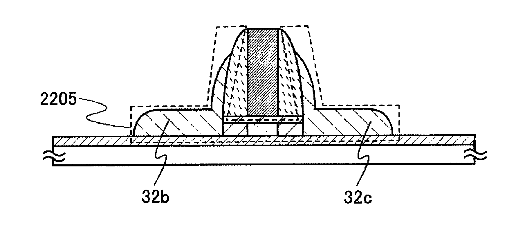
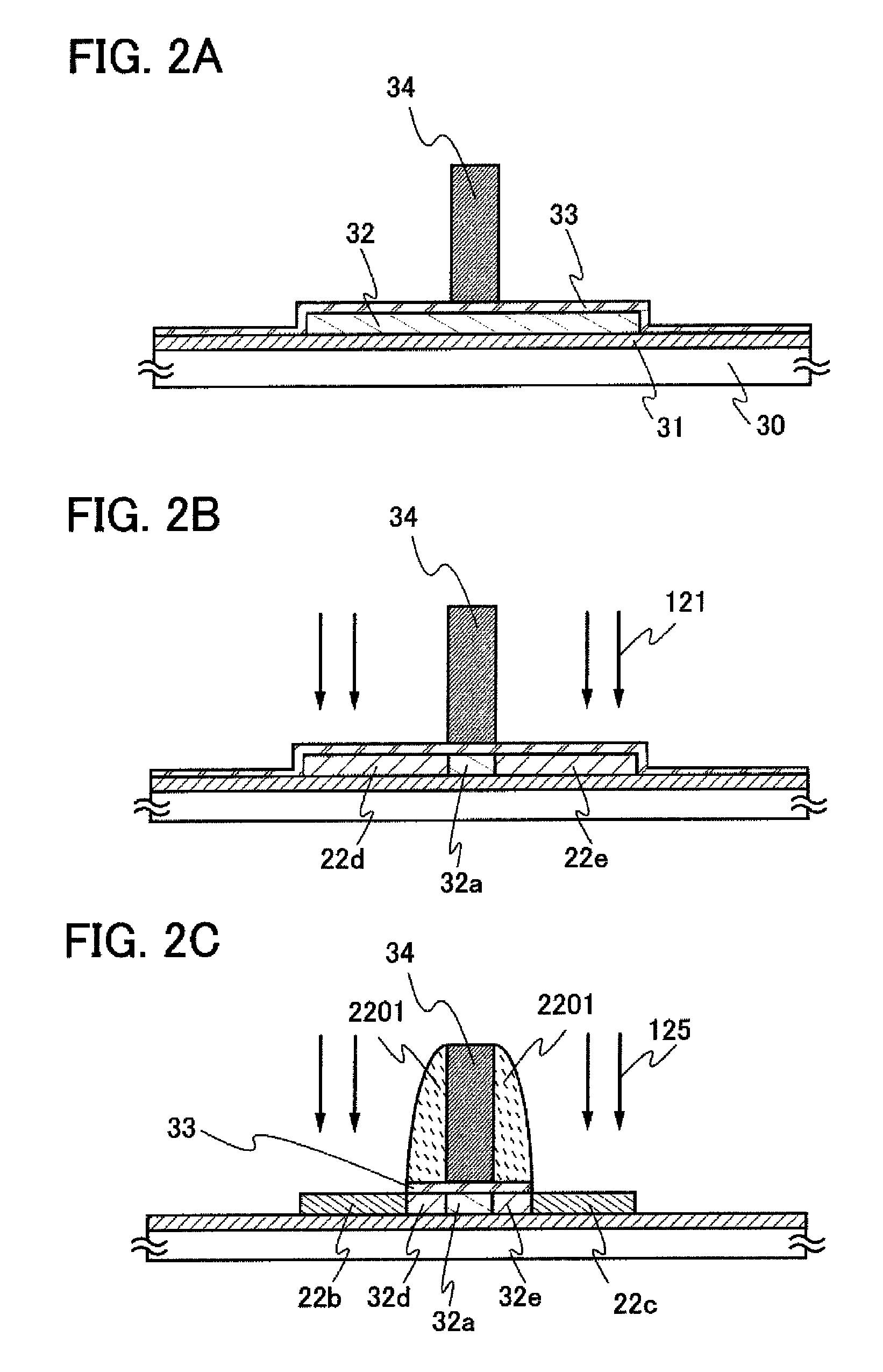
[0032]This embodiment mode will describe a structure and a manufacturing method of a semiconductor device using a semiconductor layer in which the thickness of a source region or a drain region is larger than that of a channel formation region.

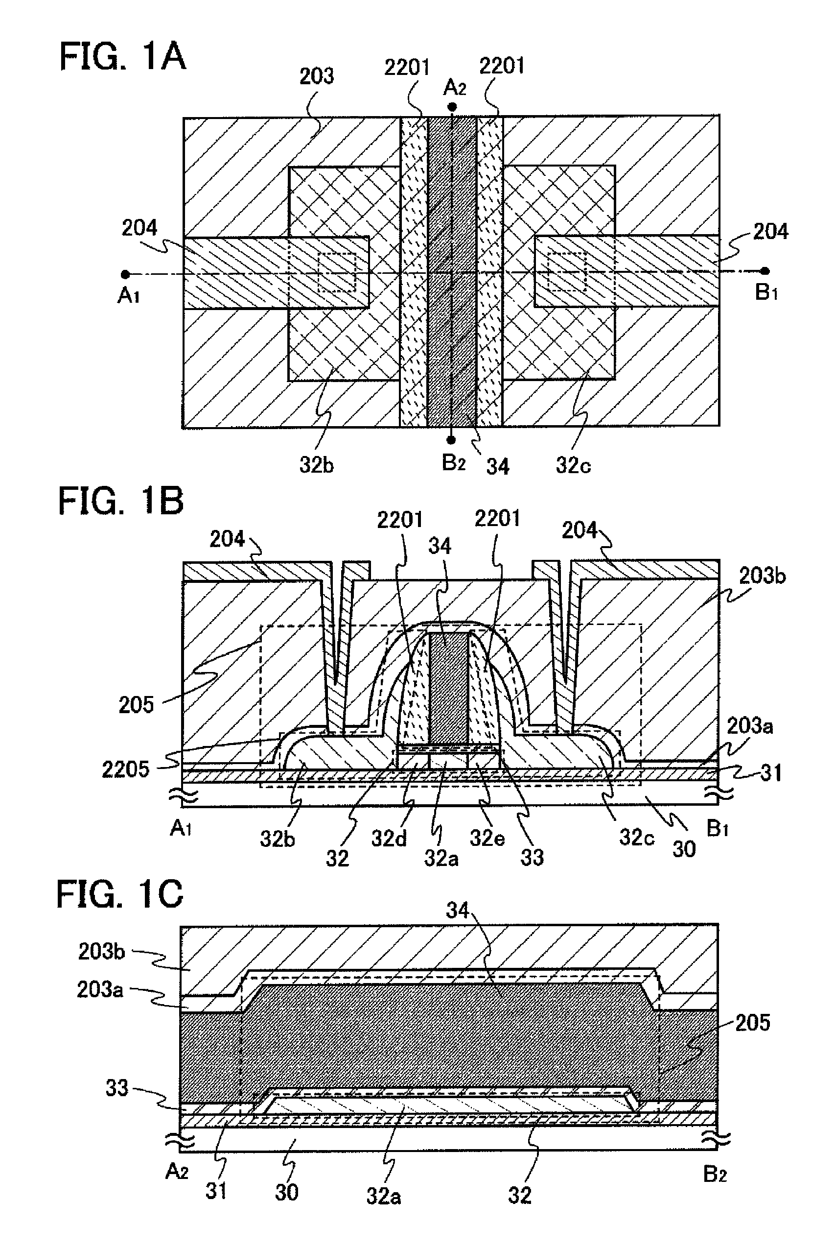
[0033]FIG. 1A is a top view and FIGS. 1B and 1C are cross-sectional views for describing a structure of a semiconductor device according to the present invention. FIG. 1A is a top view of a semiconductor device including a thin film transistor. FIG. 1B is a cross-sectional view taken along the broken line joining a dot A1 and a dot B1 in FIG. 1A and FIG. 1C is a cross-sectional view taken along the broken line joining a dot A2 and a dot B2 in FIG. 1A.

[0034]A semiconductor device described in this embodiment mode includes a thin film transistor 205 which has an insulating layer 31 formed over a substrate 30, a semiconductor layer 2205 having a first semiconductor layer 32 having an island shape and impurity regions 32b and 32c each serving as a...

embodiment mode 2

[0061]This embodiment mode will describe a semiconductor device having a different structure from that described in Embodiment Mode 1 with reference to FIGS. 5A to 6C.

[0062]FIG. 5A is a top view and FIGS. 5B and 5C are cross-sectional views for explaining a different structure of a semiconductor device according to the present invention. The semiconductor device shown in FIGS. 5A to 5C includes an insulating layer 501 which is formed over the conductive layer 34 serving as a gate electrode in addition to the structure of the semiconductor device shown in FIGS. 1A to 1C. FIG. 5A is a top view of a semiconductor device including a thin film transistor. FIG. 5B is a cross-sectional view taken along the broken line joining a dot A1 and a dot B1 in FIG. 5A and FIG. 5C is a cross-sectional view taken along the broken line joining a dot A2 and a dot B2 in FIG. 5A.

[0063]An example of a manufacturing process of a semiconductor device shown in FIGS. 5A to 5C will be described with reference t...

embodiment mode 3

[0071]This embodiment mode will describe an example of a manufacturing step of a semiconductor device using a single crystalline semiconductor layer in a channel formation region with reference to FIGS. 7A to 8D.

[0072]First, a single-crystal silicon substrate 1101 is prepared (FIG. 7A). Note that the substrate used in this embodiment mode is not limited to a single-crystal silicon substrate, and a single-crystal silicon-germanium substrate or the like may be used, as well.

[0073]Next, a silicon oxynitride (SiON) film 1102 (also referred to as a silicon oxide film that contains nitrogen) is formed over the single-crystal silicon substrate 1101 (FIG. 7A). The film thickness should be selected as appropriate by a practitioner and may be set to be from 10 nm to 500 nm, preferably, from 20 nm to 100 nm. The silicon oxynitride film 1102 functions as a part of an insulating layer of an SOI (Silicon on Insulator) substrate that is to be formed later. Note that the silicon oxynitride film 110...


PUM


Abstract

A highly responsive semiconductor device in which the subthreshold swing (S value) is small and reduction in on-current is suppressed is manufactured. A semiconductor layer in which a thickness of a source region or a drain region is larger than that of a channel formation region is formed. A semiconductor layer having a concavo-convex shape which is included in the semiconductor device is formed by the steps of forming a first semiconductor layer over a substrate; forming a first insulating layer and a conductive layer over the first semiconductor layer; forming a second insulating layer over a side surface of the conductive layer; forming a second semiconductor layer over the first insulating layer, the conductive layer and the second insulating layer; etching the second semiconductor layer using a resist formed partially as a mask; and performing heat treatment to the first semiconductor layer and the second semiconductor layer.

Description

BACKGROUND OF THE INVENTION[0001]1. Field of the Invention[0002]The present invention relates to a method for manufacturing a semiconductor device.[0003]2. Description of the Related Art[0004]In recent years, there has been extensive production of semiconductor devices in which a thin film transistor (hereinafter, also referred to as a TFT) is formed over a substrate which has an insulating surface such as a glass substrate and used as a switching element or the like. A structure of the thin film transistor has been proposed in which a semiconductor film having an island shape is formed over a substrate having an insulating surface by a CVD method, a photolithography method, or the like, and part of the semiconductor film having an island shape is used as a channel formation region of the transistor.[0005]With such a backdrop, a method for manufacturing a thin film transistor in which a subthreshold swing (here, the subthreshold swing (S value) refers to the value of a gate voltage ...

Claims


Application Information

Patent Timeline
Patent Type & Authority Patents(United States)
IPC IPC(8): H01L21/84
CPCH01L27/12H01L29/78654H01L29/66772H01L27/1266H01L29/78618H01L29/78696
Inventor OHNUMA, HIDETO
Owner SEMICON ENERGY LAB CO LTD
Why Eureka
Try Eureka