Switching circuit having low threshold voltage

a switching circuit and threshold voltage technology, applied in electronic switching, oscillator generators, pulse techniques, etc., can solve the problems of difficult to insert an additional switch formed of a semiconductor or a relay to the current path to be switched, difficult to use hemt in accordance with kawasaki et al, and difficult to replace an si transistor with a transistor formed, etc. problems, to achieve the effect of reducing on-resistance, preventing malfunction, and reducing the probability

Active Publication Date: 2010-08-24
MURATA MFG CO LTD
View PDF19 Cites 25 Cited by
  • Summary
  • Abstract
  • Description
  • Claims
  • Application Information

AI Technical Summary

Benefits of technology

[0034]Another object of the present invention is to realize reduction of on-resistance, higher speed of operation and smaller power consumption of the switching circuit for high-power main power supply, through the switching circuit and the output circuit.
[0051]As described above, according to the present invention, switching operation less prone to malfunction can be realized by using a normally-off type switching device formed of a wide band-gap semiconductor having the threshold voltage of 2V or lower. Therefore, the conventional Si power MOSFET can be replaced by the switching device formed of a wide band-gap semiconductor such as GaN, as the switching device for high-power main power supply used in an inverter of IH (Inductive Heating), an air conditioner, solar cells or a DC / DC converter. As a result, the present invention realizes reduction of on-resistance, higher speed of operation and smaller power consumption of the switching device for high-power main power supply.

Problems solved by technology

It is not easy, however, to replace an Si transistor with a transistor formed of a wide band-gap semiconductor, as the transistor formed of Si is a normally-off type device while most of the transistors formed of wide band-gap semiconductor are of normally-on type.
In such a case, the main power supply to be turned on / off by the switching device typically has a voltage of about 500V and supplies a current of about 50 A. When on / off of such high-power main power supply is to be controlled, it is difficult to insert an additional switch formed of a semiconductor or a relay to the current path to be switched.
At present, however, it is difficult to use HEMT in accordance with Kawasaki et al., as the switching device for a high-power main power supply, because such transistor has low threshold voltage, as mentioned above.
Further, because of capacitive coupling or electromagnetic coupling between the main power supply and the control circuit, high-level noise voltage also generates in the control circuit.
If the threshold voltage is low, there is a high risk that such noise voltage causes malfunction of the switching device.
When these circuits turn on / off the high voltage and high current as described above, noise voltage may be generated in the main power supply.
In addition, because of capacitive coupling or electromagnetic coupling between the main power supply and other control circuits in the apparatus, high-level noise voltage also generates in the control circuits.
At present, for a normally-off type switching device of which threshold voltage is 1V or smaller, a practical switching circuit has not yet been studied, and the problem of malfunction of the switching device caused by the noise voltage is not recognized.
Generally, when a power supply voltage of 300V or higher is used, malfunction caused by noise is possible if the threshold voltage is 2V or lower.
Such malfunction increases the risk of breakdown of FET 20, heat generation of circuit lines and fire caused by overheat of FET 20 resulting from excessive current.
This leads to possible problems such as device breakdown or fire resulting from heat generation in the circuit.
Addition of the negative voltage generating circuit having such high output and the control of the same for coordinated operation with the main power supply lead to much complicated circuit structure and hence to higher cost of the product.
Therefore, the control circuit continuously consumes power even when it is not in operation.
Further, the circuit structure would be significantly different from the conventional power MOSFET, resulting in the necessity of large-scale development of new products.

Method used


Image

  • Switching circuit having low threshold voltage
  • Switching circuit having low threshold voltage
  • Switching circuit having low threshold voltage

Examples


first embodiment

[0066]-Structure-

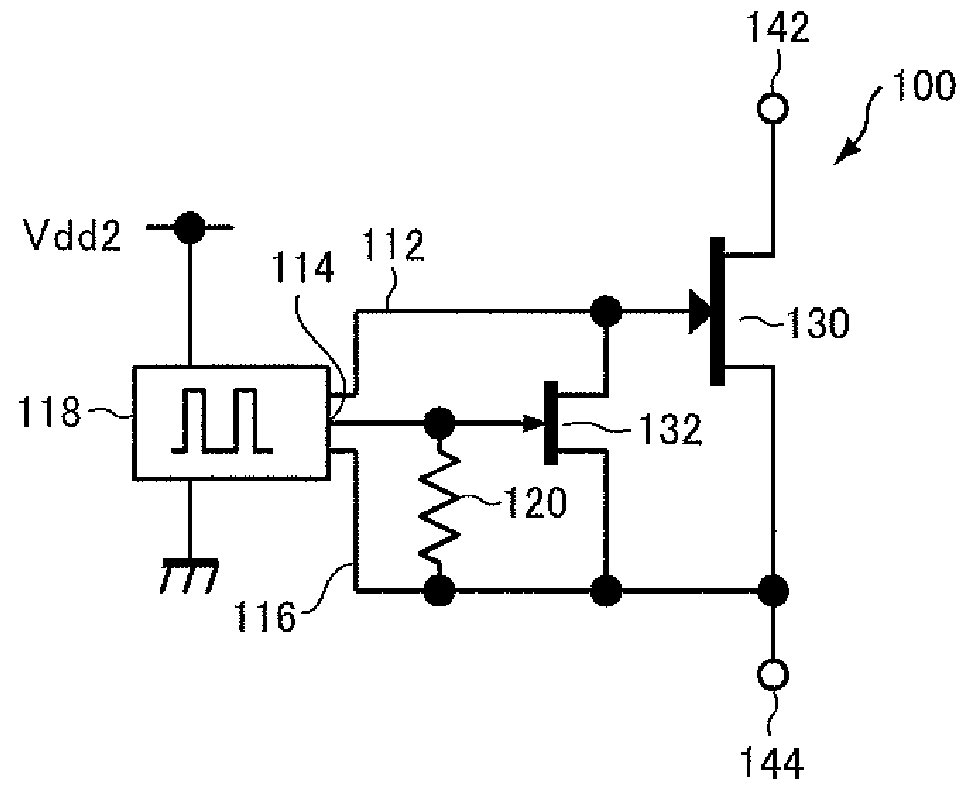
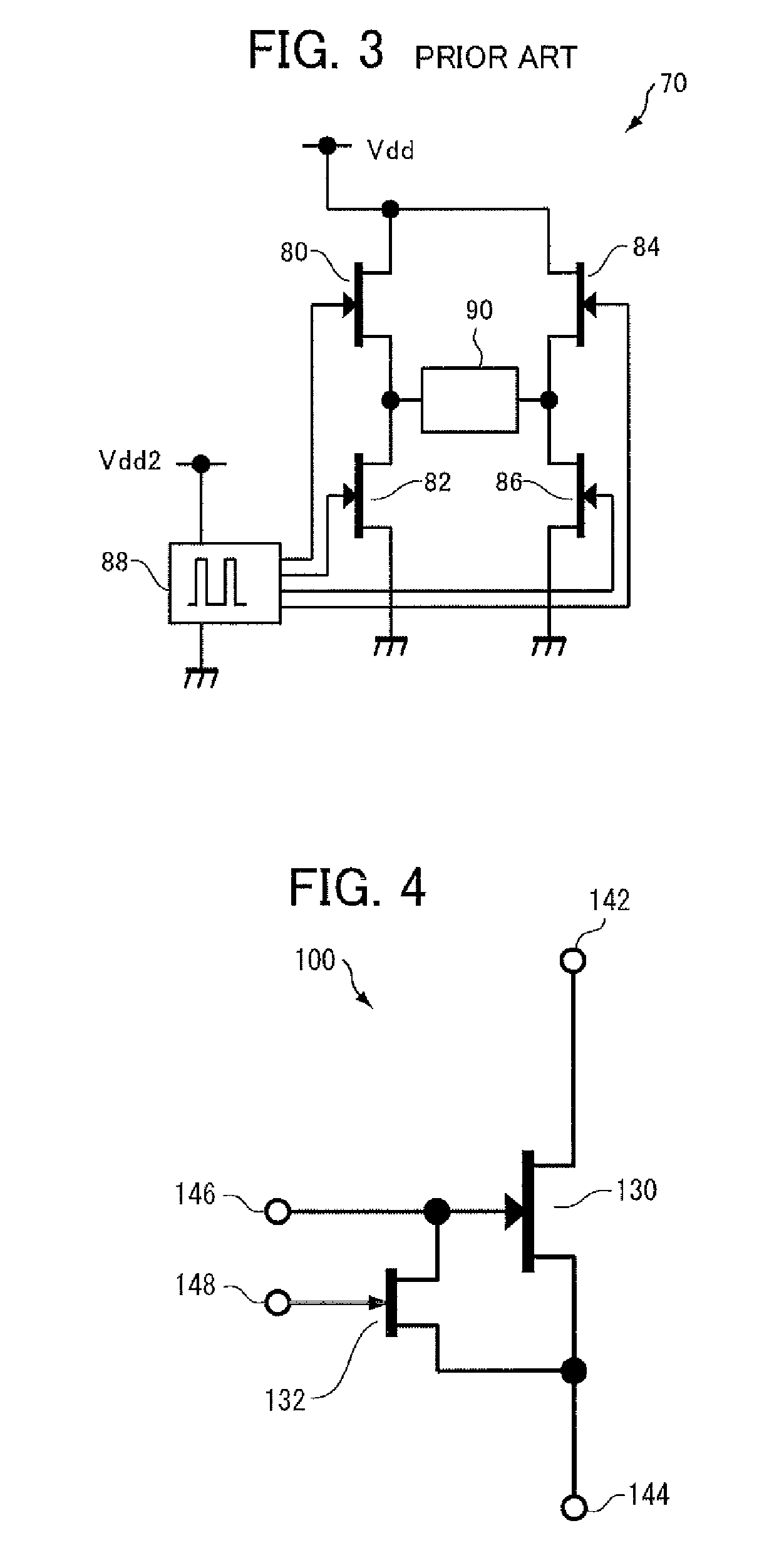
[0067]FIG. 4 shows a basic structure of a switching circuit 100 in accordance with a first embodiment of the present invention. Referring to FIG. 4, switching circuit 100 includes: a normally-off type FET 130 implemented by an AlGaN / GaN HEMT formed of a stacked structure of GaN / AlGaN, having a drain electrode 142 and a source electrode 144; and a terminal 146 connected to the gate electrode of FET 130 and receiving driving pulses for FET 130 from the outside. In the present embodiment, the threshold voltage of FET 130 is 0.3V.

[0068]Switching circuit 100 further includes: a normally-on type FET 132 having its drain electrode and source electrode connected to the gate electrode and the source electrode 144 of FET 130, respectively, and a terminal 148 connected to the gate electrode of normally-on type FET 132. Terminal 148 is for receiving a signal for stabilizing the gate potential of normally-on type FET 132, from the outside. In the present embodiment, the threshol...

second embodiment

[0083]-Structure-

[0084]FIG. 6 is a circuit diagram of a switching circuit 190 in accordance with a second embodiment of the present invention.

[0085]Referring to FIG. 6, switching circuit 190 has substantially the same structure as the switching circuit 100 shown in FIG. 5. However, it is different from switching circuit 100 shown in FIG. 5 in that it includes, in place of resistor 120 shown in FIG. 5, a normally-on type FET 200 having its source electrode and gate electrode connected commonly to the gate electrode of normally-on type FET 132 and its source electrode connected to the source electrode of normally-on type FACT 132. The gate width of the FET 200 is narrow enough to keep the current low.

[0086]- Operation-

[0087]The switching circuit 190 shown in FIG. 6 operates in the following manner.

[0088]As is well known, an FET has a characteristic similar to a very high resistance between the source / drain. Therefore, normally-on type FET 200 operates in the similar manner as resistor...

third embodiment

[0093]FIG. 7 is a circuit diagram of a switching circuit 230 in accordance with a third embodiment of the present invention.

[0094]Referring to FIG. 7, the circuit has substantially the same structure as that of the switching circuit 100 shown in FIG. 5. However, it is different from switching circuit 100 shown in FIG. 5 in that it includes, in place of resistor 120 shown in FIG. 5, a normally-off type FET 240 having its drain electrode connected to the gate electrode of normally-on type FET 132 and its source electrode and gate electrode commonly connected to the source electrode of normally-on type FET 132.

[0095]Generally, in a transistor of a GaN switching element, the threshold voltage can freely be changed by adjusting the etching time during manufacturing of the device. It is assumed that the threshold voltage Vth3 of normally-off type FET 240 and the threshold voltage Vth2 of normally-on type FET 132 are adjusted to satisfy the relation of |Vth3|2|. In the present embodiment, ...


PUM


Abstract

A switching circuit for preventing malfunction of a switching device formed of a wide band-gap semiconductor used for switching a high-power main power supply includes a normally-off type FET having a gate electrode, a source electrode connected to the ground, and a drain electrode connected to a power supply potential Vdd, and a normally-on type FET having drain and source electrodes connected to the gate and source electrodes of the FET, respectively, and a gate electrode. In the absence of any power supply, the normally-on type FET turns on. As a result, the gate / source potential of FET attains to 0V, and FET is kept off.

Description

CROSS-REFERENCE TO RELATED APPLICATION[0001]This nonprovisional application claims priority under 35 U.S.C. §119(a) on Patent Application No. 2007-250170 filed in Japan on Sep. 26, 2007, the entire contents of which are hereby incorporated by reference.BACKGROUND OF THE INVENTION[0002]1. Field of the Invention[0003]The present invention relates to a technique for improving switching of a high-power main power supply and, more specifically, to a technique for preventing malfunction of a switching device of low threshold voltage.[0004]2. Description of the Background Art[0005]Switching devices widely used these days are dominantly implemented by Si transistors. Recently, however, a device formed of a wide band-gap semiconductor such as SiC or GaN is attracting attention. The reason for this is that a wide band-gap semiconductor realizes device performance exceeding limits of physical property of Si.[0006]It is not easy, however, to replace an Si transistor with a transistor formed of ...

Claims


Application Information

Patent Timeline
Patent Type & Authority Patents(United States)
IPC IPC(8): H03K3/00
CPCH03K17/302H03K17/0406H03K17/063H03K2017/6875H03K2217/0036
Inventor KAWAMURA, HIROSHI
Owner MURATA MFG CO LTD
Why Eureka
Try Eureka