Method of controlling the film properties of PECVD-deposited thin films
a technology of pecvd and thin films, applied in plasma techniques, solid-state diffusion coatings, coatings, etc., can solve the problems of non-uniform film thickness of precursor source gas, and achieve the effect of increasing the surface area, and increasing the hollow cathode
- Summary
- Abstract
- Description
- Claims
- Application Information
AI Technical Summary
Benefits of technology
Problems solved by technology
Method used
Image
Examples
example one
PECVD Deposition of a-SiNx:H Gate Dielectric Layers by Increasing the Concentration of NH3 in the Precursor Gas Composition
[0185]We have previously described all of the performance requirements for the a-SiNx:H gate dielectric layer. We carried out extensive experimentation in an effort to produce a PECVD deposited a-SiNx:H gate dielectric layer which met the performance requirements and which provided a uniformity in film thickness and uniformity in film properties, including structural and chemical composition, when PECVD deposited over a large surface area, larger than 1000 mm×1000 mm, for example. One basic requirement is that the a-SiNx:H film deposition rate is more than 1000 Å / min, and typically more than 1300 Å / min, so that the fabrication throughput for the TFT provides adequate productivity to be economically competitive. The basic requirements for the a-SiNx:H film are that: the Si—H bonded content of the a-SiNx:H film is less than about 15 atomic %; the film stress range...
example two
PECVD Deposition of a-SiNx:H Gate Dielectric Layers of Uniform Thickness by Controlling a Combination of Process Parameters, Using the AKT™ 25 KA PECVD System
[0206]As discussed above, we have discovered that controlling a combination of PECVD deposition process parameters during deposition of silicon-containing thin film provides improved control over surface standing wave effects. These process parameters include: the spacing between the upper and lower electrodes in the plasma reactor; the RF frequency of the plasma source; the RF power to the plasma source; the process chamber pressure; and the relative concentrations of the various components in the precursor gas composition.
[0207]We performed a series of experiments to determine the advantageous ranges for each process parameter, in order to provide maximum control over surface standing wave effects and uniformity of film properties (especially film thickness). A comparison between film uniformity available prior to the present...
example three
Modification of the Diffuser Plate of the Gas Distribution Assembly
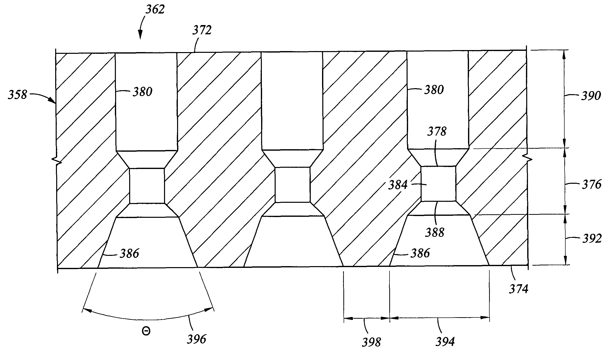
[0223]We found that, as substrate sizes increased over 30,000 cm2, to 40,000 cm2 and beyond, process modifications such as those described in Examples One and Two, above, are not always enough to compensate for surface standing wave effects. For example, FIG. 20 is a graph 2000 of the film thickness 2002 as a function of the distance of travel 2004 (in mm) across the width of the substrate, where the width of the substrate was 2200 mm and the length of the substrate was 1870 mm (for a total substrate area of 41,140 cm2), for an a-SiNx:H film. The a-SiNx:H film was PECVD deposited in an AKT™ 40 K PECVD System (which is described above in “APPARATUS FOR PRACTICING THE INVENTION” and shown schematically in FIGS. 19A-19C) process chamber having an electrode spacing of 600 mils, using a “standard” (uniform hollow cathode cavity) diffuser plate.
[0224]We discovered that controlling the plasma density at point locations on t...
PUM
| Property | Measurement | Unit |
|---|---|---|
| equivalent radius | aaaaa | aaaaa |
| thickness | aaaaa | aaaaa |
| temperature | aaaaa | aaaaa |
Abstract
Description
Claims
Application Information


