Metal schemes of trench MOSFET for copper bonding

a copper bonding and trench mosfet technology, applied in semiconductor devices, semiconductor/solid-state device details, electrical devices, etc., can solve the problems of increased cost, increased cost, and introduction of bad wire bonding adhesion issues, so as to reduce the damage of cu wire bonding to semiconductor devices and reduce the cost

Active Publication Date: 2010-08-31
FORCE MOS TECH CO LTD
View PDF2 Cites 7 Cited by
  • Summary
  • Abstract
  • Description
  • Claims
  • Application Information

AI Technical Summary

Benefits of technology

[0012]It is therefore an object of the present invention to provide new and improved trench MOSFET cell and manufacture process to minimize the Cu wire bonding damage to semiconductor device without additional cost.
[0013]One aspect of the present invention is that, a W layer with a resistance reduction layer composed of Ti or Ti / N whereon underneath a front metal of source and gate is provided as buffer layer for reducing Cu wire bonding damage. The difference between the prior art of U.S. Pat. No. 6,888,196 and the present invention is that, in the prior art the W layer is totally removed from surface of oxide interlayer film after W deposition to fill the source-body contact trench while in the present invention it is selectively removed, in other words, the W layer is only kept on the oxide interlayer surface of the areas underneath source and gate metal to serve as buffer layer when bonding Cu wire upon source and gate metal, therefore, no additional cost is needed. And, comparing to structure in FIG. 1, the high wire bonding resistance and wire bonding adhesion issue are both resolved due to Cu bonding wire directly bonded to front source and gate metal layer. Additionally, contact resistance between buffer layer and front metal of source and gate are further reduced by employing the resistance reduction layer composed of Ti or Ti / N sandwiched therebetween.
[0014]Another aspect of the present invention is that, in some preferred embodiment, an improved source-body contact structure is proposed, which has vertical contact trench sidewalls within oxide interlayer and N+ source regions, and has slope contact trench sidewalls within P-body region. To be detailed, the contact trench sidewalls are substantially vertical (90+ / −5 degree) within oxide interlayer and N+ source regions, and the taper angle is less than 85 degree respect to top surface of epitaxial layer within P-body region. By employing this structure, the P+ area can be enlarged to wrap the bottom and the slope sidewalls of source-body contact trench in P-body region, which resolves the high Rp problem and enhances the avalanche capability. On the other hand, there will be no BF2 Ion Implantation into the sidewalls of N+ source regions because the sidewall are substantially vertical, avoiding the N+ concentration reduction issue occurs in FIG. 4, thus preventing the increasing of source contact resistance from happening.
[0015]Another aspect of the present invention is that, in some preferred embodiment, the conventional poly gate within gate trench is replaced by a terrace gate, which will provide additional poly over silicon mesa area to further reduce gate resistance Rg, and what is the most important is that, a self-aligned source contact is implemented by employing the terrace gate structure, therefore resolved avalanche current Iav and Rds non-uniform distribution issue resulted from misalignment between contact and trench.
[0016]Briefly, in a preferred embodiment, as shown in FIG. 5, the present invention disclosed a trench MOSFET cell comprising: a heavily doped substrate of a first semiconductor doping type, e.g., N dopant, with a layer of Ti / Ni / Ag on the rear side serving as drain metal; a lighter doped epitaxial layer of a first semiconductor doping type grown on said substrate; a plurality of trenches etched into said epitaxial layer as gate trenches; a gate oxide layer along the inner surface of said gate trenches; doped poly filled within said gate trenches to form trench gates; a thin oxide layer formed onto trench gate and the top surface of epitaxial layer; body regions of a second semiconductor doping type, e.g., P dopant, extending between every two trench gates; source regions above the top surface of P-body regions; an oxide interlayer film onto front surface of a thin oxide layer; a vertical source-body contact trench penetrating through said oxide interlayer, said source regions and into said body regions with vertical sidewalls; P+ area wrapping the bottom of source-body contact trench to reduce the resistance between source and body; W metal deposited over a layer of Ti / TiN or Co / TiN to serve as contact metal plug into source-body contact trench and also serve as buffer layer covering the surface of the oxide interlayer; metal Al alloys or Copper over Ti or Ti / TiN layer deposited onto a resistance reduction layer composed of Ti or Ti / N to serve as source and gate metal with Cu wires bonded whereon.

Problems solved by technology

By employing non-conductive passivation material as buffer layer, the structure of prior art shown in FIG. 1 minimized bonding damage on semiconductor device, however, comparing to its advantage, the disadvantages brought by this passivation structure are more significant to a certain extent.
First of all, more cost are needed due to the requirement of additional passivation layer deposition, masking and etching; Second, wire bonding resistance is increased because that some Cu bonding area is occupied by the non-conductive passivation layer; Third, bad wire bonding adhesion issue is introduced due to Cu wire contacting with passivation layer in some area.
Therefore, thick front source metal is required to minimize the bonding damage to semiconductor device, leading to extra cost and metal etching complication.
Therefore, the conventional vertical source contact shown in FIG. 2 also has a poor avalanche capability which significantly affects the performance of whole device.
However, even if the slope contact trench is helpful to enlarge the P+ area under trench source-body contact during BF2 Ion Implantation, it is still not enough to resolve the high Rp problem as the P+ area is also formed only around the bottom of source-body contact trench.
However, anther problem is thus introduced, which is that the N+ concentration on contact trench sidewalls will be reduced as a result of compensation by BF2 Ion Implantation due to no oxide film as stopper, causing high source contact resistance.

Method used


Image

  • Metal schemes of trench MOSFET for copper bonding
  • Metal schemes of trench MOSFET for copper bonding
  • Metal schemes of trench MOSFET for copper bonding

Examples


Embodiment Construction

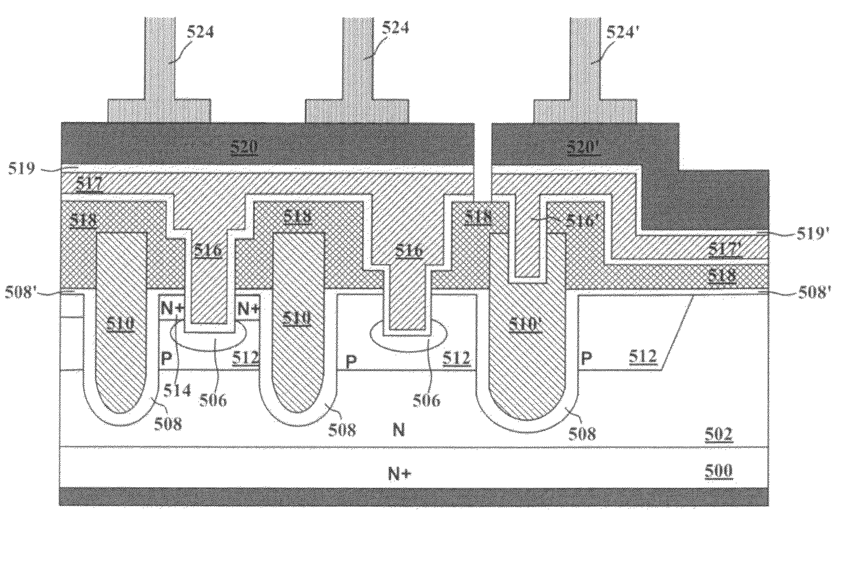
[0032]Please refer to FIG. 5 for a preferred embodiment of the present invention. The shown trench MOSFET cell is formed on an N+ substrate 400 coated with back metal Ti / Ni / Ag 422 on rear side as drain. Onto said substrate 400, grown an N epitaxial layer 402, and a plurality of trenches were etched wherein. To fill these trenches, doped poly was deposited into trenches above gate oxide layer 408 to form trench gates 410. P-body regions 412 are extending between trenches gates 410 with a layer of source regions 414 above the top surface of P-body regions 412. Source-body contact trench is etched through an oxide interlayer 418, a thin oxide layer 408′ and N+ source region 414, and into P-body region 412. Especially, the sidewalls of source-body contact trench are perpendicular to the front surface of epitaxial layer. To fill source-body contact trench, Ti / TiN / W or Co / TiN / W is deposited not only within contact trench as metal plug 416 but also cover the surface of oxide interlayer 418...


PUM

PropertyMeasurementUnit
angleaaaaaaaaaa
angleaaaaaaaaaa
taper angleaaaaaaaaaa

Abstract

A trench MOSFET with improved metal schemes is disclosed. The improved contact structure applies a buffer layer to minimize the bonding damage to semiconductor when bonding copper wire upon front source and gate metal without additional cost.

Description

BACKGROUND OF THE INVENTION[0001]1. Field of the Invention[0002]This invention relates generally to the cell structure and fabrication process of power semiconductor devices. More particularly, this invention relates to a novel and improved cell structure and improved process for fabricating a trench MOSFET with improved metal schemes for copper bonding.[0003]2. The Prior Arts[0004]Please refer to FIG. 1 for a Cu bonding compatible bond pad structure of prior art (U.S. Patent application publication No. 20080006951). The disclosed structure includes a buffering structure comprising exposed electrode metal regions 118 of electrode metal layer 114 formed over a TiNi barrier metal layer 112 and non-conductive passivation regions 120 having same material as passivation layer 116. As illustrated, while bonding Cu bonding wire 122, some of the passivation regions 120 were pushed into the electrode metal layer 114 to provide a buffer function to keep Cu bonding wire 122 away from barrier m...

Claims


Application Information

Patent Timeline
Patent Type & Authority Patents(United States)
IPC IPC(8): H01L29/72
CPCH01L24/05H01L24/06H01L24/49H01L29/41741H01L29/41766H01L29/456H01L29/66727H01L29/66734H01L29/7811H01L29/7813H01L2924/1306H01L2224/0603H01L2924/01033H01L2924/13091H01L2924/04941H01L24/45H01L29/1095H01L29/4236H01L2224/04042H01L2224/05559H01L2224/45147H01L2224/4845H01L2224/48463H01L2224/494H01L2924/01005H01L2924/01013H01L2924/01014H01L2924/01015H01L2924/01022H01L2924/01027H01L2924/01028H01L2924/01029H01L2924/01047H01L2924/0105H01L2924/01074H01L2924/01082H01L2924/00014H01L2924/00H01L2224/4911H01L24/48
Inventor HSIEH, FU-YUAN
Owner FORCE MOS TECH CO LTD
Why Eureka
Try Eureka