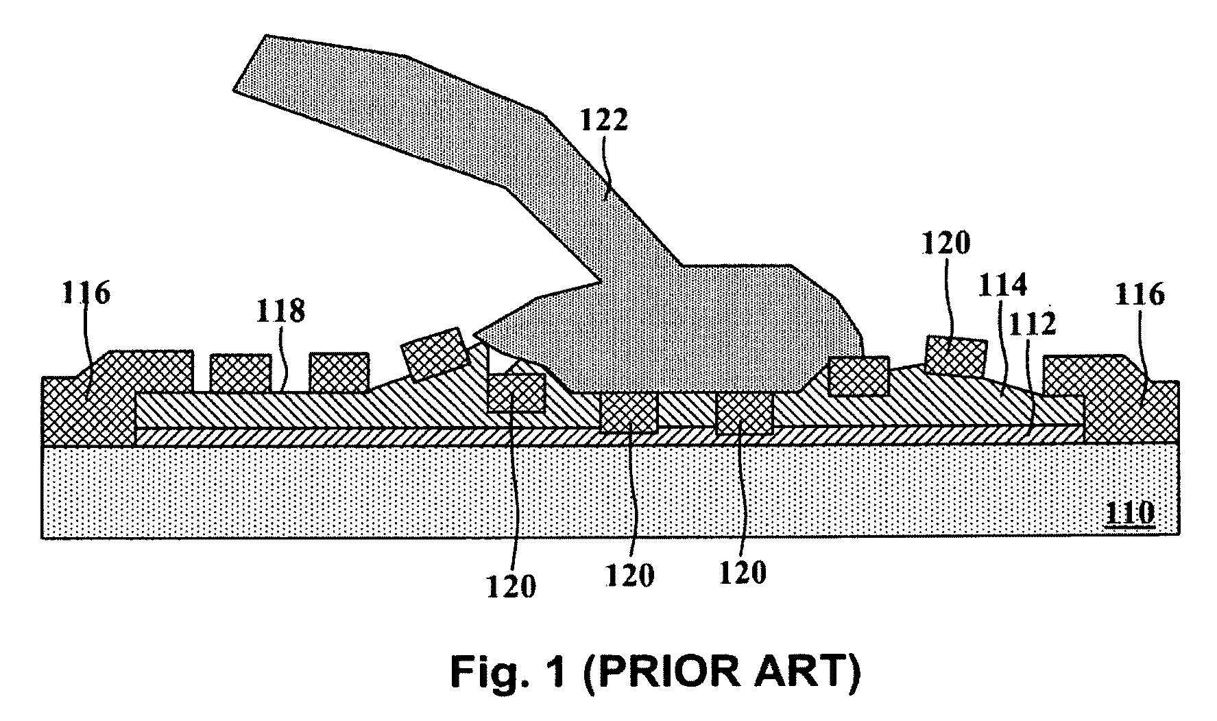
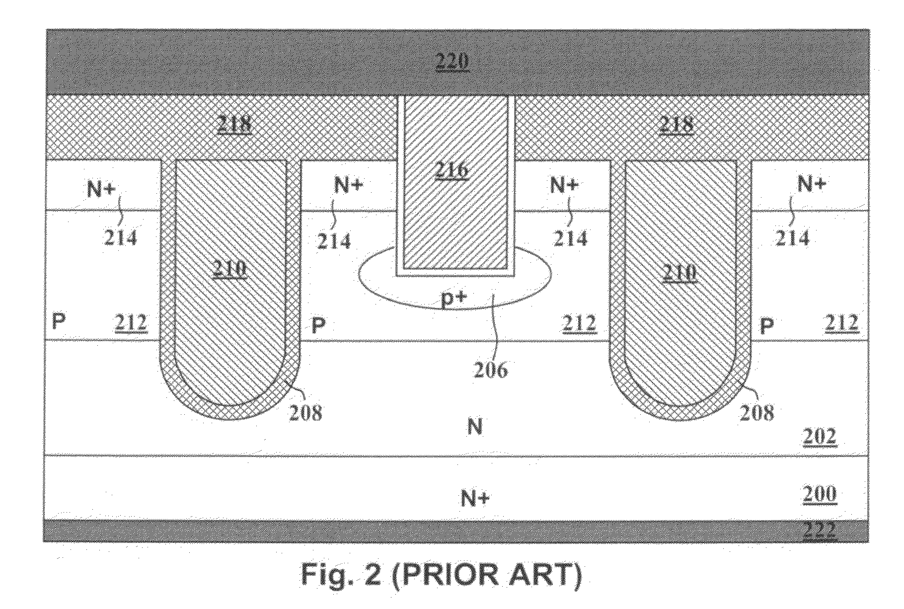
[0013]One aspect of the present invention is that, a W layer with a resistance reduction layer composed of Ti or Ti / N whereon underneath a front metal of source
and gate is provided as buffer layer for reducing Cu wire bonding damage. The difference between the prior art of U.S. Pat. No. 6,888,196 and the present invention is that, in the prior art the W layer is totally removed from surface of
oxide interlayer film after W deposition to fill the source-
body contact trench while in the present invention it is selectively removed, in other words, the W layer is only kept on the
oxide interlayer surface of the areas underneath source
and gate metal to serve as buffer layer when bonding Cu wire upon source and gate metal, therefore, no additional cost is needed. And, comparing to structure in FIG. 1, the high wire bonding resistance and wire bonding adhesion issue are both resolved due to Cu bonding wire directly bonded to front source and gate metal layer. Additionally,
contact resistance between buffer layer and front metal of source and gate are further reduced by employing the resistance reduction layer composed of Ti or Ti / N sandwiched therebetween.
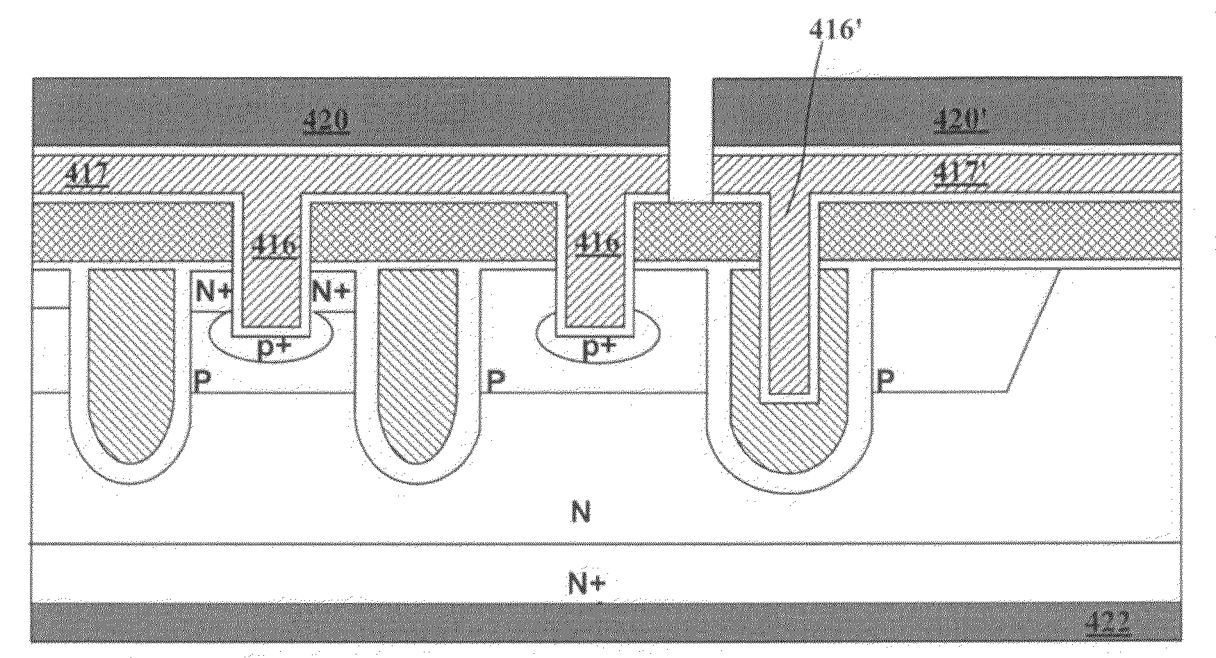
[0014]Another aspect of the present invention is that, in some preferred embodiment, an improved source-body contact structure is proposed, which has vertical contact trench sidewalls within oxide interlayer and N+ source regions, and has slope contact trench sidewalls within P-
body region. To be detailed, the contact trench sidewalls are substantially vertical (90±5 degree) within oxide interlayer and N+ source regions, and the taper angle is less than 85 degree respect to top surface of epitaxial layer within P-
body region. By employing this structure, the P+ area can be enlarged to wrap the bottom and the slope sidewalls of source-body contact trench in P-
body region, which resolves the high Rp problem and enhances the avalanche capability. On the other hand, there will be no BF2
Ion Implantation into the sidewalls of N+ source regions because the sidewall are substantially vertical, avoiding the N+ concentration reduction issue occurs in FIG. 4, thus preventing the increasing of source
contact resistance from happening.
[0015]Another aspect of the present invention is that, in some preferred embodiment, the conventional poly gate within gate trench is replaced by a terrace gate, which will provide additional poly over
silicon mesa area to further reduce
gate resistance Rg, and what is the most important is that, a self-aligned source contact is implemented by employing the terrace gate structure, therefore resolved avalanche current Iav and Rds non-uniform distribution issue resulted from misalignment between contact and trench.
[0016]Briefly, in a preferred embodiment, as shown in FIG. 5, the present invention disclosed a trench
MOSFET cell comprising: a heavily doped substrate of a first semiconductor
doping type, e.g., N
dopant, with a layer of Ti / Ni / Ag on the rear side serving as drain metal; a lighter doped epitaxial layer of a first semiconductor
doping type grown on said substrate; a plurality of trenches etched into said epitaxial layer as gate trenches; a
gate oxide layer along the inner surface of said gate trenches; doped poly filled within said gate trenches to form trench gates; a
thin oxide layer formed onto
trench gate and the top surface of epitaxial layer;
body regions of a second semiconductor
doping type, e.g., P
dopant, extending between every two trench gates; source regions above the top surface of P-
body regions; an oxide interlayer film onto front surface of a
thin oxide layer; a vertical source-body contact trench penetrating through said oxide interlayer, said source regions and into said
body regions with vertical sidewalls; P+ area wrapping the bottom of source-body contact trench to reduce the resistance between source and body; W metal deposited over a layer of Ti /
TiN or Co /
TiN to serve as contact metal plug into source-body contact trench and also serve as buffer layer covering the surface of the oxide interlayer; metal Al alloys or
Copper over Ti or Ti /
TiN layer deposited onto a resistance reduction layer composed of Ti or Ti / N to serve as source and gate metal with Cu wires bonded whereon.

