Method and system for the examination of specimen

a specimen and system technology, applied in the field of specimen examination, can solve the problems of inability to provide accurate critical dimensions, accurate height or edge width measurements without the need of massive manual interference, and inability to accurately register the elements of a stereo image pair, so as to achieve the effect of reducing the number of specimens, and reducing the amount of specimens

Active Publication Date: 2010-09-21
APPLIED MATERIALS INC
View PDF11 Cites 6 Cited by
  • Summary
  • Abstract
  • Description
  • Claims
  • Application Information

AI Technical Summary

Benefits of technology

[0009]By providing an oblique angle of incidence on the one hand and a corresponding movement of specimen on the other hand, stereo images of a specimen can be produced in a fast and reliable manner without the need for any additional alignments and without the need for excessive image processing. Accordingly, the additional information, which is contained in stereo images and which is extremely valuable in many cases, can be accessed without causing any additional costs.
[0011]It has been found by the present inventors that the chromatic aberrations caused by the first step of the deflection can be compensated to a large extent by the second step of the deflection if the two deflections are properly adjusted. The combined action of the two step deflection and focussing of the beam then leads to a resolution in the range of a few nanometers, which is comparable with the resolution that can be achieved without providing an oblique angle of incidence. The invention has thus the advantage that large angles of incidence on a specimen can be provided without a reduction in resolution arising from large chromatic aberrations.
[0012]According to a still further aspect of the present invention, methods are provided that allow an accurate measurement of important distances on the surface of a specimen, especially on the surface on a semiconductor wafer. These methods use a tilted beam of charged particles to get the information in a very fast and reliable manner.

Problems solved by technology

The resolution of the conventional optical microscopy is limited by the wavelength of the visible light.
These two limitations have led to the increased popularity of charged particle devices for the examination of specimen.
Thereby, the device is actually located within the production environment, so that problems of the wafer processing are recognized as soon as possible.
However, conventional charged particle devices are not capable of providing accurate critical dimension, accurate height or accurate edge width measurements without the need of massive manual interference.
However, mechanically tilting the specimen leads to a number of disadvantages.
Due to mechanical imperfections a lateral movement of the specimen is inevitable which often results in misregistrations between the elements of a stereo image pair.
Furthermore, tilting large specimen, for example a 12 inch semiconductor wafer, requires a very robust and costly mechanical configuration in order to guarantee an adequate resistance of such a stage against vibrations.
However, the height resolution of the proposed systems lies in the range of 75 to 100 nm, which is not sufficient for the requirements of the semiconductor industry.
However, using an atomic force microscope requires an additional experimental setup which increases the costs significantly and is also very slow.

Method used


Image

  • Method and system for the examination of specimen
  • Method and system for the examination of specimen
  • Method and system for the examination of specimen

Examples


Embodiment Construction

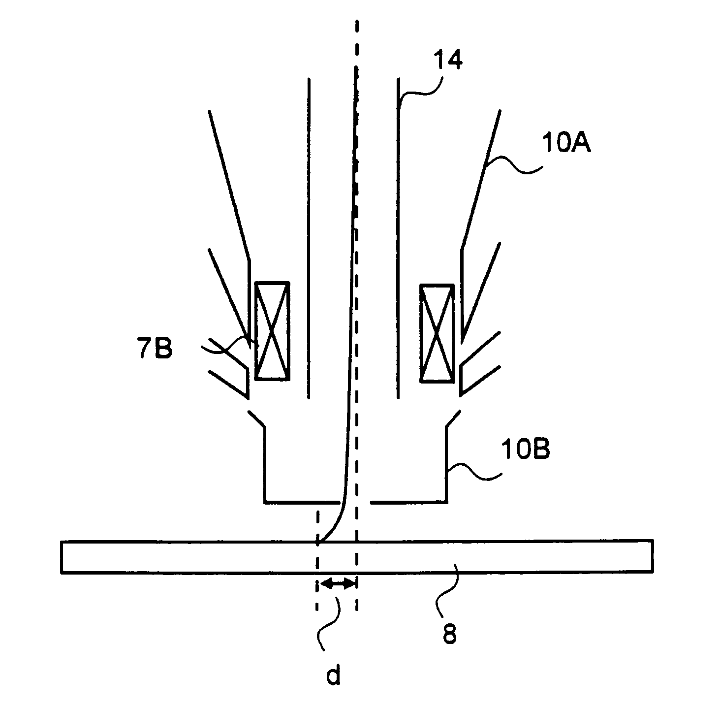
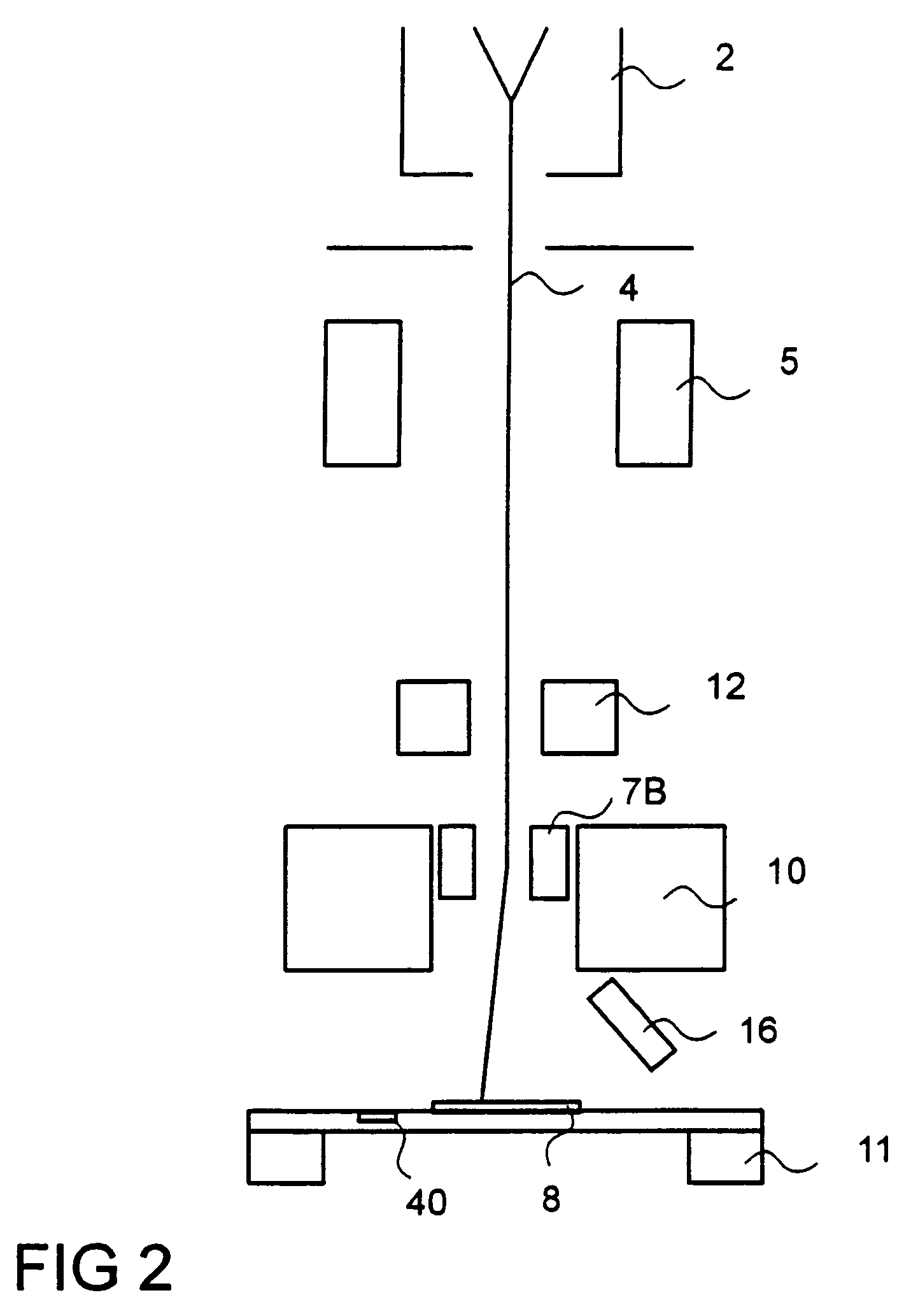
[0024]Preliminary, it should be appreciated by those skilled in the art that the present invention can be used with any charged particle device. However, for convenience the invention will be described with respect to its implementation in a scanning electron microscope (SEM). A preferred embodiment according to the invention is shown schematically in FIG. 1. The basic components of the device are an electron source 2, a lens system (condenser lens 5 and objective lens 10), scanning coils 12, beam shift coils 7A and a detector 16. In operation an electron beam 4 is emitted from the electron source 2. The electron source may, for example, be a tungsten-hairpin gun, a lanthanum-hexaboride gun, or a field-emission gun. The electrons are accelerated by an accelerating voltage supplied to the electron source 2. Since the beam diameter produced directly by the electron source usually is too large to generate a sharp image at high magnification, the electron beam 4 is guided through the co...


PUM

PropertyMeasurementUnit
angle of incidenceaaaaaaaaaa
energyaaaaaaaaaa
distanceaaaaaaaaaa

Abstract

The present invention provides, according to a first aspect, a method for the examination of specimen with a beam of charged particles. The method provides one or more images of the specimen made with different view angles, so that, compared to a single image of the specimen, a lot of additional information about the specimen can be accessed. The different view angles (angles of incidence) are achieved by tilting the beam between the two images and moving the specimen to a new position so that the displacement of the beam caused by the tilting of the beam is compensated. Accordingly, while displaying / recording the second image the beam scans over the same area as it has scanned while displaying / recording the first image.

Description

RELATED APPLICATIONS[0001]The present application is a continuation of application Ser. No. 10 / 390,979, entitled “Method and System For The Examination of Specimen”, filed on Mar. 17, 2003, which is a continuation of application Ser. No. 10 / 149,565, filed Jun. 11, 2002, now abandoned. This patent application is hereby incorporated by reference in its entirety.FIELD OF THE INVENTION[0002]The invention relates to a method and a system for the examination of specimen. Especially, the invention relates to a method and a system for the examination of specimen with a beam of charged particles.BACKGROUND OF THE INVENTION[0003]The resolution of the conventional optical microscopy is limited by the wavelength of the visible light. Furthermore, at the highest resolution the conventional optical microscopy has a very shallow depth of field. These two limitations have led to the increased popularity of charged particle devices for the examination of specimen. Compared to optical light accelerat...

Claims


Application Information

Patent Timeline
Patent Type & Authority Patents(United States)
IPC IPC(8): G01B15/04G01N23/203G01N23/22G21K7/00
CPCG01N23/203G01N23/22H01J37/1478H01J37/265H01J2237/202H01J2237/2611H01J2237/281
Inventor GOLDENSHTEIN, ALEXBEN-AV, RADELPEARL, ASHERPETROV, IGORHAAS, NADAVADAMEC, PAVELGOLD, YARON
Owner APPLIED MATERIALS INC
Why Eureka
Try Eureka