

Method for forming metal film by ALD using beta-diketone metal complex
a metal complex and metal film technology, applied in the direction of resistive material coating, liquid/solution decomposition chemical coating, superimposed coating process, etc., can solve the problems of difficult to form good wirings, discontinuous cu films formed by pvd method on top of these barrier films, and difficult to form barrier films having a uniform thickness. , to achieve the effect of low resistance, high shielding property and easy adsorption on the substra
- Summary
- Abstract
- Description
- Claims
- Application Information
AI Technical Summary
Benefits of technology
Problems solved by technology
Method used
Image

Examples
example 1
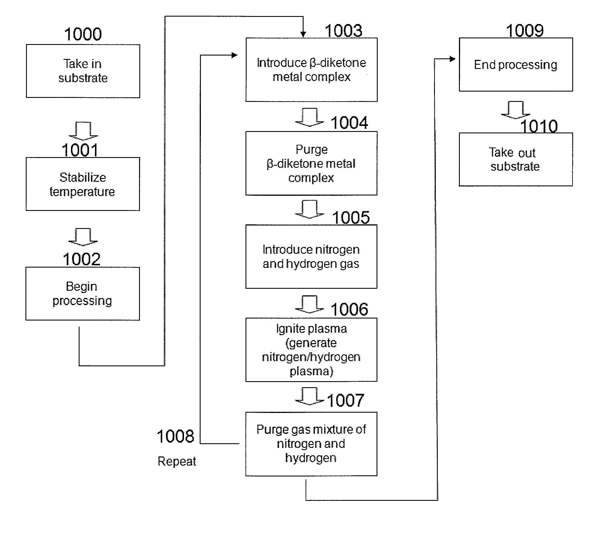
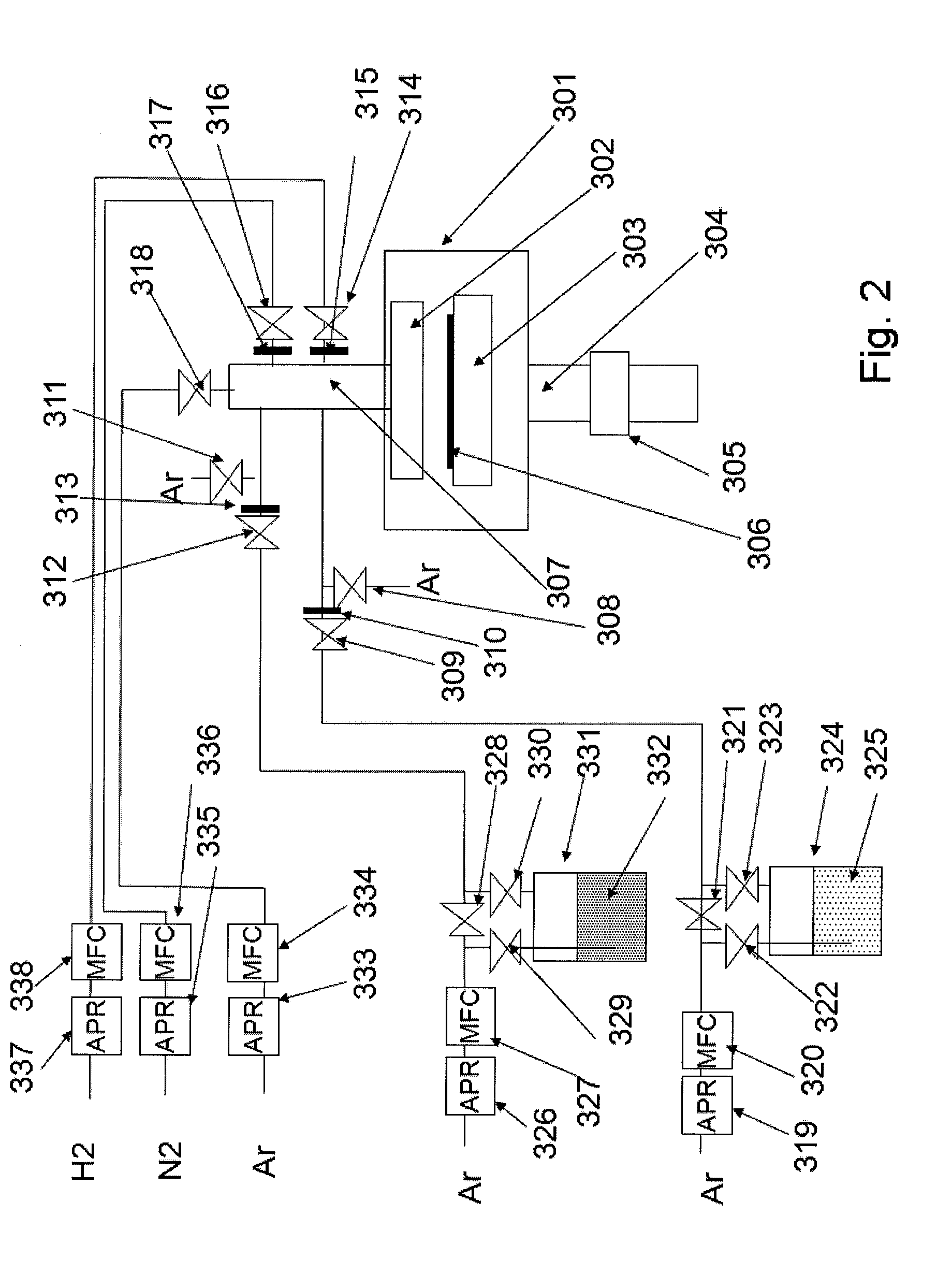
[0173]In this example, a process of forming a Co film is illustrated. Using the ALD apparatus shown in FIG. 2, an inter-layer connection structure using a Co film was formed according to the steps shown in FIGS. 3A to 3F.
[0174]In FIG. 2, the heating base 303 in the processing chamber 301 was set to 300° C. The Co material 325, or tridipivaloylmathanatocobalt (DPM3CO), was filled in a bottle 324 and this bottle was heated to 120° C. This Co material 325 had a vapor pressure of 0.5 torr, and vapor of the Co material was supplied by an argon carrier gas to a substrate via a valve 309 and orifice 310. After the Co material was supplied for 1 to 3 seconds, or desirably 1 second, this Co material was purged by the argon gas supplied from a valve 318, after which N2 was supplied by 50 sccm from a valve 316 and orifice 317, followed by the supply of H2 by 200 sccm from a valve 314 and orifice 315. High frequency power of 200 to 500 W and 13.56 MHz was then applied to this mixture gas and th...
example 2
[0177]In this example, an inter-layer connection structure was formed through the procedure shown in FIGS. 5A to 5F using a process of forming Ru and Cu films continuously in the same reaction chamber. In the ALD apparatus shown in FIG. 2, one material 325 is a Ru material containing β-diketone ligands, while the other material 332 is a Cu material containing β-diketone ligands.
[0178]A substrate was transferred to the reaction chamber, and first in FIG. 2 the heating base 303 in the processing chamber 301 was set to 300° C. The Ru material, or tridipivaloylmathanatoruthenium (DPM3Ru) 325, was filled in a bottle 324, and this bottle was heated to 120° C. This Ru material 325 had a vapor pressure of 0.1 torr, and vapor of the Ru material was supplied by an argon carrier gas to the substrate via a valve 309 and orifice 310. After the Ru material was supplied for 5 to 10 seconds, or desirably 5 seconds, this Ru material was purged by the argon gas supplied from a valve 318, after which ...
example 3
[0183]This example illustrates a process of forming a RuTaN film as a Cu barrier layer and then forming Ru and Cu layers. In the ALD apparatus shown in FIG. 2, one material 325 is a Ru material containing β-diketone ligands, while the other material 332 is a Ta organic metal material.
[0184]A substrate was transferred to the reaction chamber, and first in FIG. 2 the heating base 303 in the processing chamber 301 was set to 300° C. The Ta material, or TAIMATA (tertiaryamylimidotris(dimethylamido)tantalum), was supplied for 1 second. Taimata was supplied by an Ar carrier gas from a bottle 331 heated to 80° C. Next, 50 sccm of N2 was supplied from a valve 316 and orifice 317, and 200 sccm of H2 was supplied from a valve 314 and orifice 315. High frequency power of 200 to 500 W and 13.56 MHz was then applied to this mixture gas and the excited plasma was used to break down the Taimata adsorbed onto the substrate into Ta atoms. Although the plasma application time varies depending on the ...
PUM
| Property | Measurement | Unit |
|---|---|---|
| frequency | aaaaa | aaaaa |
| thickness | aaaaa | aaaaa |
| temperature | aaaaa | aaaaa |
Abstract
Description
Claims
Application Information