Gate strip with reduced thickness

a gate strip and thickness reduction technology, applied in the field of metal-oxide-semiconductor devices, can solve the problems of low polysilicon gate dopant concentration in metal-oxide-semiconductor devices, adversely containing p-type dopants, and conventional pre-doping process, etc., to improve device matching, reduce inter-diffusion of pre-doping impurities, and improve threshold voltage control

Active Publication Date: 2010-10-12
TAIWAN SEMICON MFG CO LTD
View PDF3 Cites 3 Cited by
  • Summary
  • Abstract
  • Description
  • Claims
  • Application Information

AI Technical Summary

Benefits of technology

[0013]The advantageous features of the embodiments of the present invention include reduced inter-diffusion of pre-doped impurities in gate electrodes of MOS devices, improved threshold voltage control, improved device matching, and the ability for further down-scaling integrated circuits.

Problems solved by technology

However, such reductions result in lower polysilicon gate dopant concentrations in metal-oxide-semiconductor (MOS) devices.
The conventional pre-doping process, however, suffers limitations. FIG. 1 illustrates a cross-sectional view of an intermediate stage in a conventional pre-doping process.
After the patterning of polysilicon layer 10 and dielectric layer 8, the gate poly of a resulting NMOS device will adversely contain p-type dopants, and the gate poly of a resulting PMOS device will adversely contain n-type dopants.
The adversely diffused dopants neutralize portions of the desired dopants, causing the fluctuation in threshold voltages.
The above-discussed problem becomes worse in small-scale integrated circuits.
The problem will increase in severity if lower-scale technologies are used.
Therefore, this problem limits the improvement in future device performance and device optimization.

Method used


Image

  • Gate strip with reduced thickness
  • Gate strip with reduced thickness
  • Gate strip with reduced thickness

Examples


Embodiment Construction

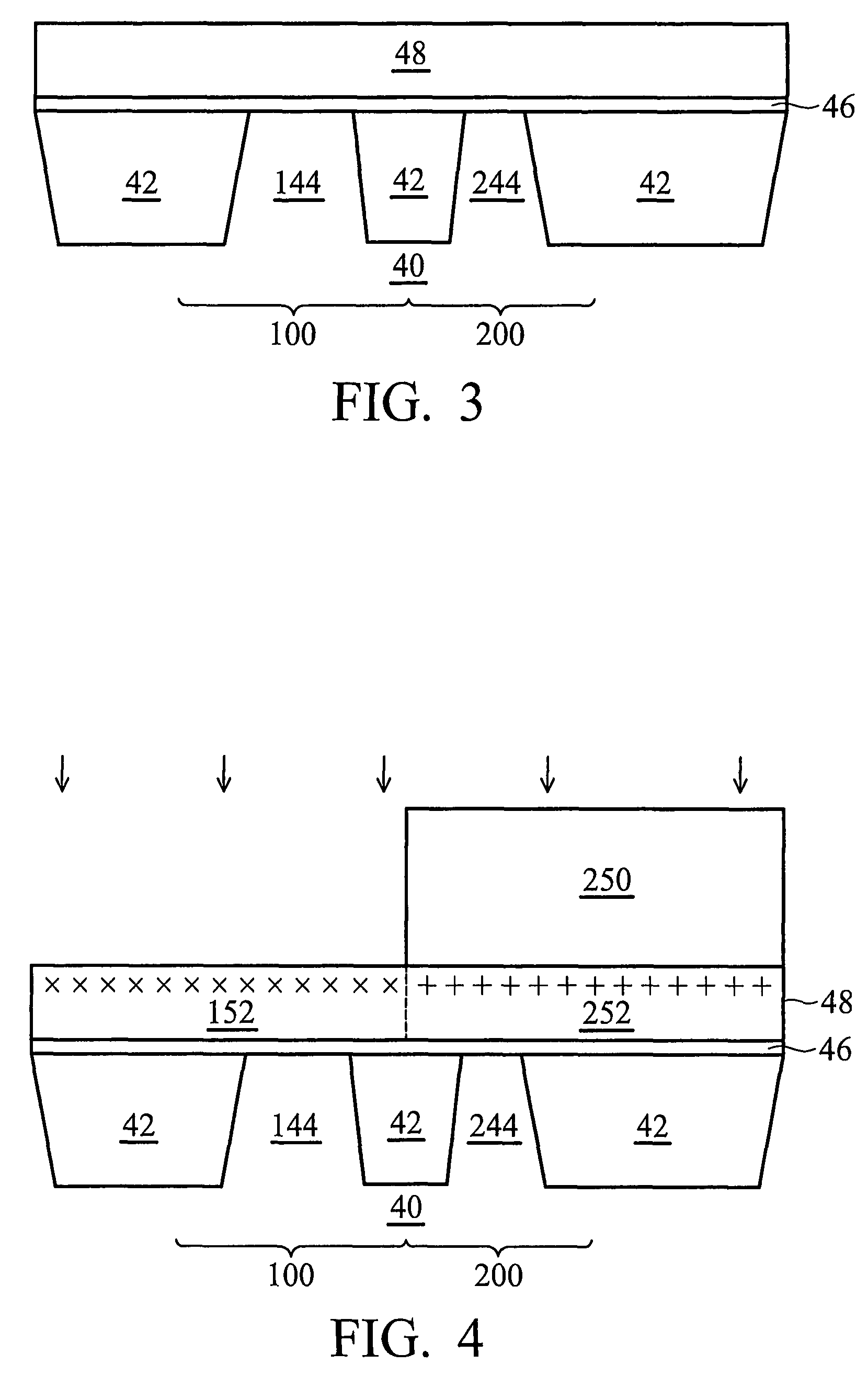
[0018]The making and using of the presently preferred embodiments are discussed in detail below. It should be appreciated, however, that the present invention provides many applicable inventive concepts that can be embodied in a wide variety of specific contexts. The specific embodiments discussed are merely illustrative of specific ways to make and use the invention, and do not limit the scope of the invention.

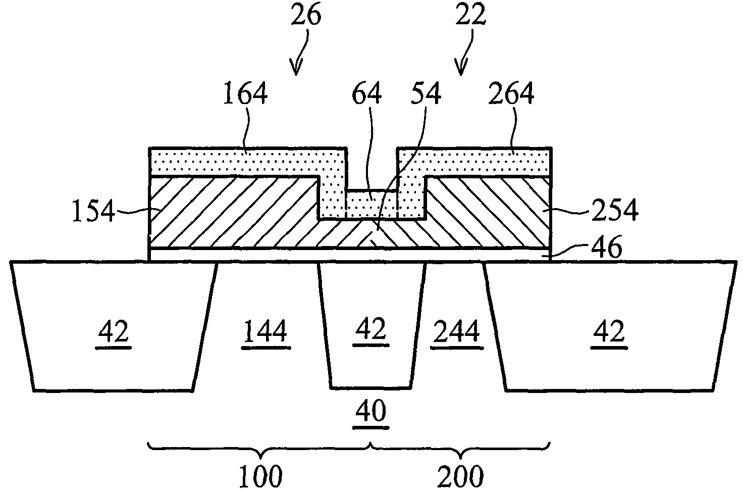
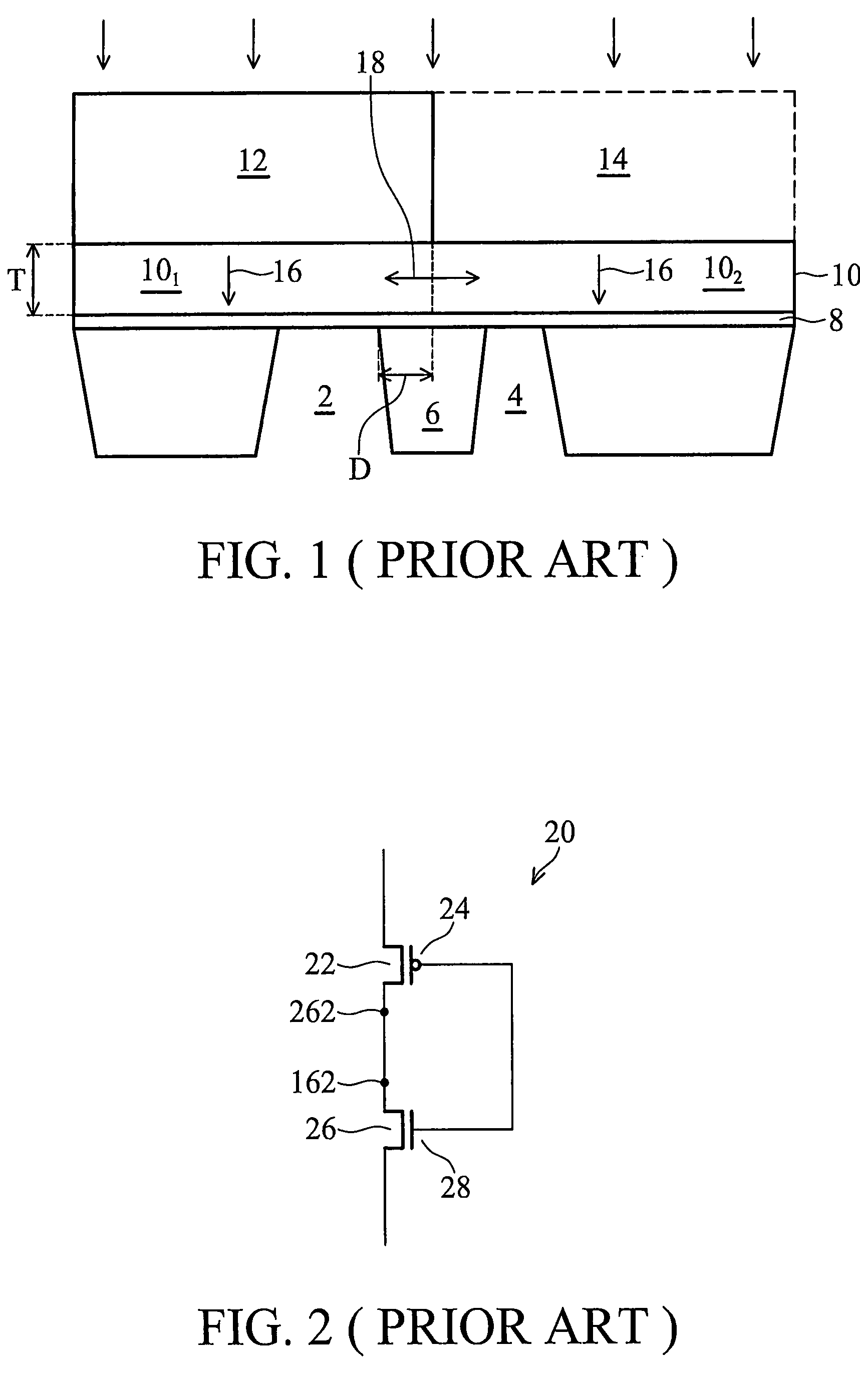
[0019]FIG. 2 illustrates a circuit diagram of an exemplary circuit 20, which includes a p-type metal-oxide-semiconductor (PMOS) device 22 connected to an n-type MOS (NMOS) device 26. Gate 24 of PMOS device 22 is connected to gate 28 of NMOS device 26. Drain 262 of PMOS device 22 is connected to drain 162 of NMOS device 26. Circuit 20 is commonly used in inverters, static random access memory cells, and the like. It is to be noted that circuit 20 is only an example used for explaining the concept of the present invention, and the concept of the present invention can be applied...


PUM


Abstract

A semiconductor structure with reduced inter-diffusion is provided. The semiconductor structure includes a semiconductor substrate; a first well region in the semiconductor substrate; a second well region in the semiconductor substrate; an insulating region between and adjoining the first and the second well regions; a gate dielectric layer on the first and the second well regions; and a gate electrode strip on the gate dielectric and extending from over the first well region to over the second well region. The gate electrode strip includes a first portion over the first well region, a second portion over the second well region, and a third portion over the insulating region. A thickness of the third portion is substantially less than the thicknesses of the first and the second portions.

Description

TECHNICAL FIELD[0001]This invention relates generally to semiconductor devices, and more particularly to metal-oxide-semiconductor devices and methods for forming the same.BACKGROUND[0002]In integrated circuit formation technologies, thermal budget, dopant concentration and dopant depth of source and drain regions are continuously reduced for short channel effect improvement. However, such reductions result in lower polysilicon gate dopant concentrations in metal-oxide-semiconductor (MOS) devices. When the dopant concentration in a polysilicon gate is lower than a threshold value, a depletion layer is induced at the interface between the polysilicon gate and the underlying gate dielectric, resulting in an increased effective dielectric thickness and a degraded saturation current.[0003]In order to solve this problem, a pre-gate doping process was commonly used for improving the performance of MOS devices. In a typical pre-gate doping process, after the formation, but before the patte...

Claims


Application Information

Patent Timeline
Patent Type & Authority Patents(United States)
IPC IPC(8): H01L23/48
CPCH01L21/823475H01L21/823871H01L21/82345H01L21/823842
Inventor LIAW, JHON-JHY
Owner TAIWAN SEMICON MFG CO LTD
Why Eureka
Try Eureka