System-on-a-chip and power gating circuit thereof

a technology of power gating circuit and system on a chip, which is applied in the direction of pulse technique, electrical pulse generator details, instruments, etc., can solve the problems of error actions of function blocks, voltage fluctuation of the source line in the chip, index growth of sub-threshold leakage current, etc., and achieve the effect of reducing a transient curren

Inactive Publication Date: 2010-11-09
IND TECH RES INST
View PDF11 Cites 21 Cited by
  • Summary
  • Abstract
  • Description
  • Claims
  • Application Information

AI Technical Summary

Benefits of technology

[0009]The present invention is directed to a power gating circuit capable of reducing a transient current generated by the power gating circuit.
[0013]The present invention uses the charge pump circuit to change the bulk voltage of the first transistor of the power gating circuit, so as to modulate a threshold voltage of the first transistor to reduce the transient current when the transistor is conducted by increasing the threshold voltage, and further to suppress the voltage fluctuation of the entire SOC. The hold circuit restores the threshold voltage of the first transistor to a normal value at a predetermined rate, such that the power gating circuit when restoring the normal operating state may provide larger current, and the entire SOC may operate normally. Therefore, the present invention may prevent error actions of the entire SOC caused by an over large transient current.

Problems solved by technology

Therefore, in order to maintain the overall performance of the circuit, threshold voltages of transistors must be lowered, which will lead to an indexed growth of the sub-threshold leakage current.
However, in FIG. 1, the gate voltage of each PMOS transistor will generate a large transient current during the transition (e.g., changing from a high voltage level to a low voltage level), and the self-inductance generated by the large transient current flowing through the bonding wires and the parasitic inductance in the chip will cause voltage fluctuation of the source line in the chip.
If the amplitude of the voltage fluctuation is great, the internal circuit of the function block 120 is often locked at a wrong value, or the circuit transit at a wrong time point, leading to error actions of the function block 120.
However, though the power gating circuit reduces the transient current by conducting the transistors step by step, all the transistors are fully on when being conducted, so the transient current of the power gating circuit is still quite large.
However, though the power gating circuit can suppress the voltage fluctuation, the circuit structure is too complicated.

Method used


Image

  • System-on-a-chip and power gating circuit thereof
  • System-on-a-chip and power gating circuit thereof
  • System-on-a-chip and power gating circuit thereof

Examples


Embodiment Construction

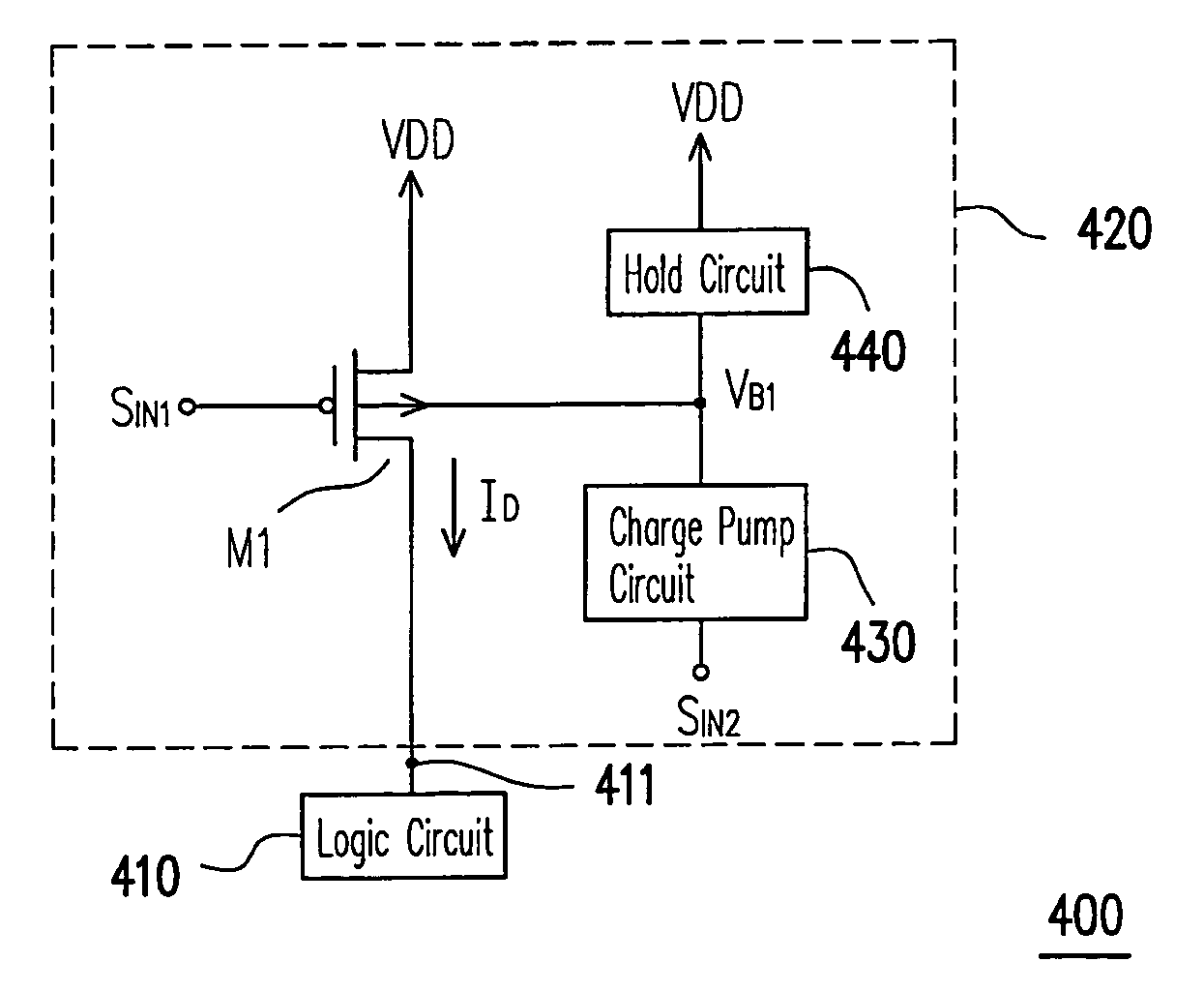
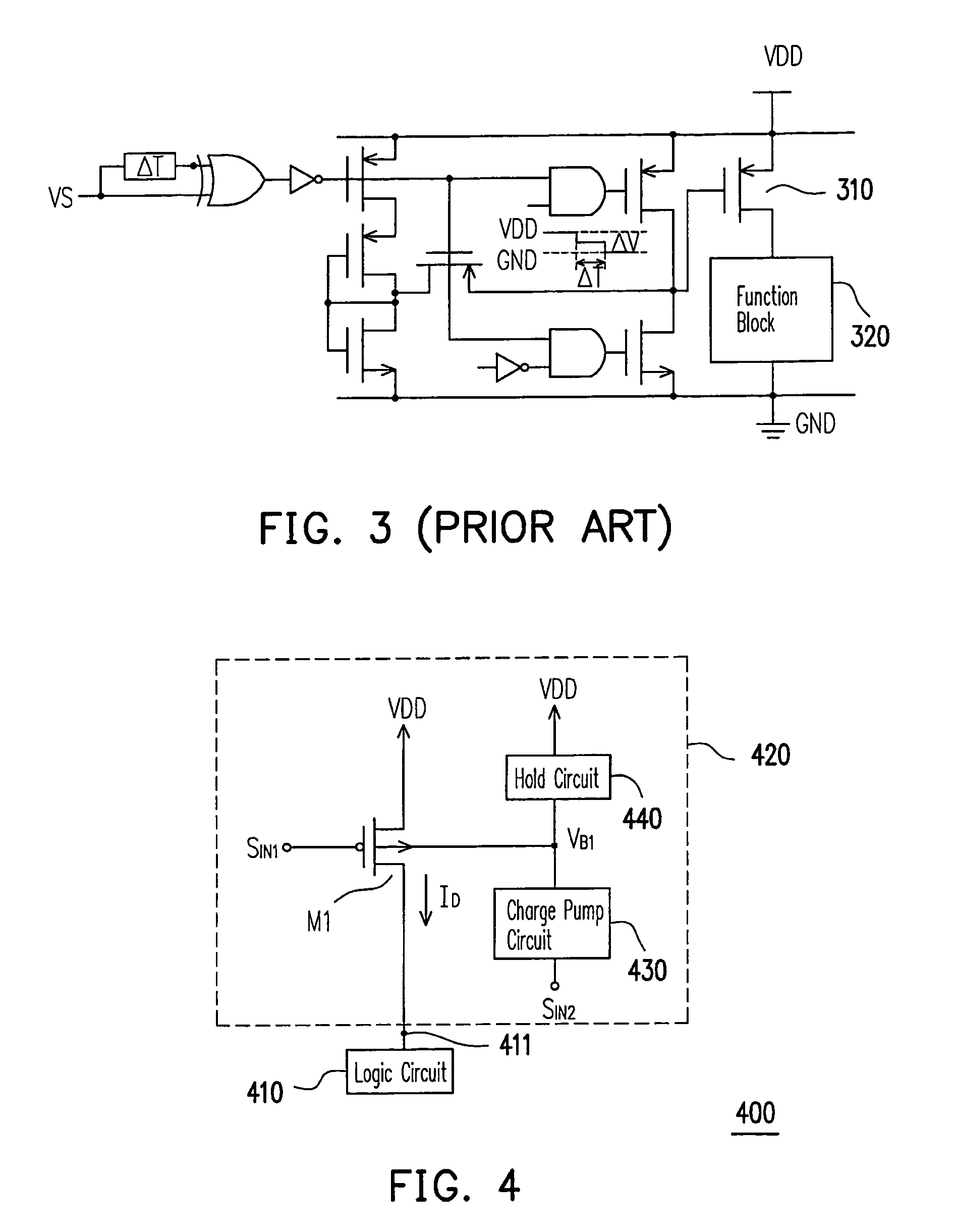
[0050]FIG. 4 is a block diagram of an SOC according to an embodiment of the present invention. Referring to FIG. 4, the SOC 400 includes a logic circuit 410 and a power gating circuit 420. The logic circuit 410 has a power terminal 411 for receiving power required for the logic circuit 410 to operate. Through the control of a first input signal SIN1, a first voltage (e.g., a system voltage VDD) is determined whether or not to pass through the power gating circuit 420 to serve as an output voltage, so as to provide the operating power required by the logic circuit 410. Therefore, the SOC 400 can selectively turn off the logic circuit 410, so as to reduce the power consumption of the SOC 400.

[0051]The power gating circuit 420 includes a first transistor M1, a charge pump circuit 430, and a hold circuit 440. In this embodiment, the first transistor M1, for example, is a PMOS transistor. A first source / drain terminal of the first transistor M1 is coupled to the first voltage (e.g., the ...


PUM


Abstract

A system-on-a-chip and a power gating circuit thereof are provided. The power gating circuit includes a first transistor, a charge pump circuit, and a hold circuit. A gate terminal of the first transistor is controlled by a first input signal. A first source / drain terminal of the first transistor is coupled to a first voltage. A second source / drain terminal of the first transistor outputs an output voltage. The charge pump circuit is coupled to a bulk terminal of the first transistor for changing a bulk voltage of the first transistor according to a second input signal. The hold circuit is coupled to the bulk terminal of the first transistor for holding the bulk voltage of the first transistor.

Description

CROSS-REFERENCE TO RELATED APPLICATION[0001]This application claims the priority benefit of Taiwan application serial no. 96137467, filed on Oct. 5, 2007. The entirety of the above-mentioned patent application is hereby incorporated by reference herein and made a part of this specification.BACKGROUND OF THE INVENTION[0002]1. Field of the Invention[0003]The present invention relates to a system-on-a-chip and a power gating circuit thereof.[0004]2. Description of Related Art[0005]Currently, the system-on-a-chip (SOC) applied in telecommunication products or computers is developing in the trend of high performance and portability, so its power consumption has become an important consideration in design. The most effective way to reduce the power consumption of a circuit is to reduce the operating voltage of the circuit. However, if the operating voltage is lowered, the overall performance of the circuit will be lowered accordingly. Therefore, in order to maintain the overall performanc...

Claims


Application Information

Patent Timeline
Patent Type & Authority Patents(United States)
IPC IPC(8): G05F3/02
CPCH03K17/163H03K19/0016H03K2217/0018
Inventor CHANG, CHUNG-YUHUANG, CHING-JI
Owner IND TECH RES INST
Why Eureka
Try Eureka