Process for making interconnect solder Pb-free bumps free from organo-tin/tin deposits on the wafer surface

a technology of interconnect solder and pb, which is applied in the direction of machine/engine, manufacturing tools, and soldering apparatus, etc., can solve the problems of organo-sn and sn

Inactive Publication Date: 2010-11-16
ULTRATECH INT INC
View PDF13 Cites 6 Cited by
  • Summary
  • Abstract
  • Description
  • Claims
  • Application Information

AI Technical Summary

Problems solved by technology

The process however may result in organo-Sn and Sn or other components of the solder being deposited on the surface of the wafer during transfer processing.
These wafers will be rejected due to these surface deposits because the presence of these deposits is a source of high resistance shorts between C4's and paths for electro-migration fails during field use.

Method used


Image

  • Process for making interconnect solder Pb-free bumps free from organo-tin/tin deposits on the wafer surface
  • Process for making interconnect solder Pb-free bumps free from organo-tin/tin deposits on the wafer surface
  • Process for making interconnect solder Pb-free bumps free from organo-tin/tin deposits on the wafer surface

Examples


Embodiment Construction

)

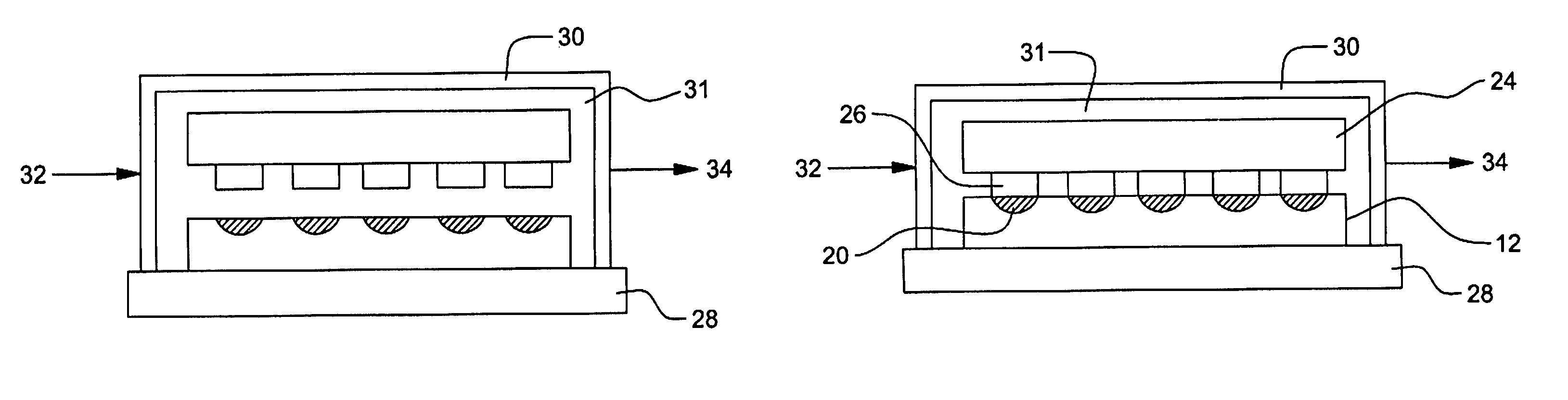
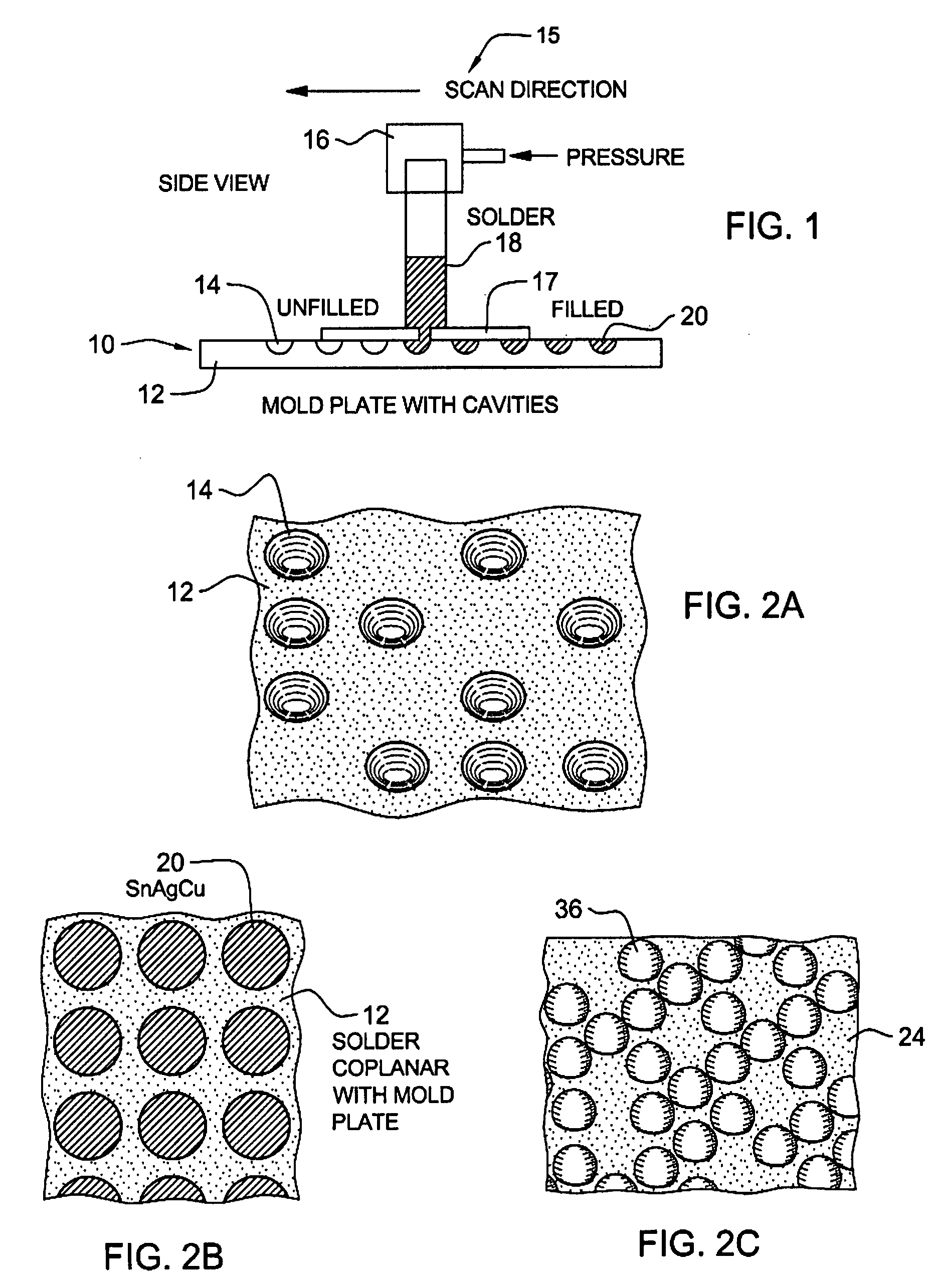
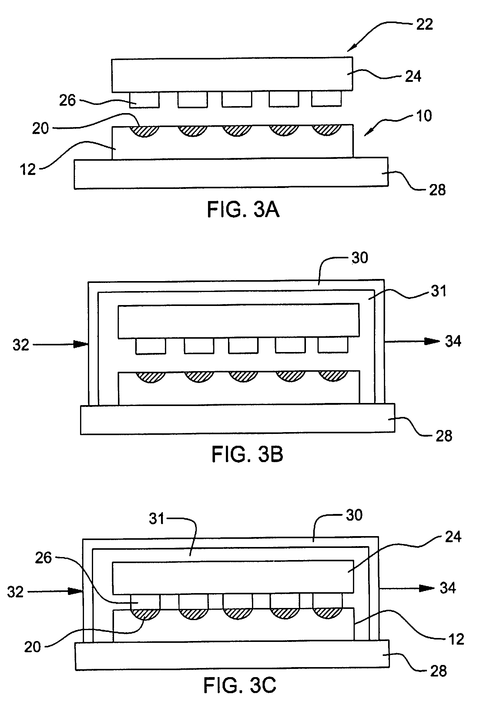
[0043]In describing the preferred embodiment of the present invention, reference will be made herein to FIGS. 1-4E of the drawings in which like numerals refer to like features of the invention.

[0044]Various solders may be readily processed using the method of the invention and these include lead and lead-free ternary and quaternary alloys. Lead-free alloys are of particular commercial significance and for convenience the following description will be directed to such lead-free alloys although it will be appreciated by those skilled in the art that any suitable solder may be readily processed using the method of the invention. Exemplary lead-free alloys include Sn-1.8% Ag, Sn-0.5% Ag and Sn-0.7% Cu. Also, in particular, the following description will be directed to tin containing lead-free alloys since these are likewise of significant commercial interest and an efficient method of providing solder interconnects with these alloys is of important commercial consideration.

[0045]IMS i...


PUM

PropertyMeasurementUnit
distanceaaaaaaaaaa
distanceaaaaaaaaaa
temperatureaaaaaaaaaa

Abstract

A method is provided for making of interconnect solder bumps on a wafer or other electronic device without depositing any significant amount of tin or other solder component from the solder onto the wafer surface which tin can cause shorts or other defects in the wafer. The method is particularly useful for well-known C4NP interconnect technology. In one aspect of the invention, a reducing gas flow rate is used to remove oxides from the solder surfaces and wafer pad surfaces and is of a sufficient determined or pre-determined flow and / or chamber or mold / wafer spacing to provide a gas velocity across the solder surfaces and wafer pad surfaces so that Sn or other contaminants do not deposit on the wafer surface during solder transfer. In another aspect, the transfer contact is performed below the melting point of the solder and subsequently heated to above the melting temperature while in transfer contact. The heated solder in contact with the wafer pads is transferred to the wafer pads.

Description

BACKGROUND OF THE INVENTION[0001]1. Field of the Invention[0002]The present invention relates to the making of interconnect solder bumps on a wafer or other electronic device without depositing any significant amount of tin from the solder onto the wafer surface which tin can cause shorts or other defects in the wafer, and, in particular, to the well-known C4NP interconnect technology.[0003]2. Description of Related Art[0004]Forming an electronic package assembly whereby an electrical component such as an integrated circuit chip is electrically and mechanically connected to a substrate, a card, or board, another chip or another electronic part is well-known in the art. This technology is generally termed surface mount technology (SMT) and has gained acceptance as the preferred means of making electronic package assemblies. The interconnect technology is commonly known as ball grid array packaging, C4 flip chip interconnect, multi-chip modules, multilayer and micro via printed wiring...

Claims


Application Information

Patent Timeline
Patent Type & Authority Patents(United States)
IPC IPC(8): H01L21/44H01L21/00B23K31/00B23K31/02
CPCB23K3/0623B23K2201/40B23K2101/40
Inventor KNICKERBOCKER, SARAH H.ALLEN, SEAN A.GARANT, JOHN J.GORRELL, JERRY A.PALMATIER, PHILLIP WTESSLER, CHRISTOPHER L
Owner ULTRATECH INT INC
Why Eureka
Try Eureka