Tunnel field-effect transistors with superlattice channels

a tunnel-effect transistor and super-lattice channel technology, applied in the field of tunnel-effect transistors with superlattice channels, can solve the problems of sacrificing source-drain leakage current, unable to achieve fast switching of ultra-thin-body mosfets on soi or finfet devices, and unable to achieve fast switching at low operation voltage for future nanometer devices. achieve the effect of reducing gate leakage current, improving on-current, and reducing the curren

Inactive Publication Date: 2010-11-16
TAIWAN SEMICON MFG CO LTD
View PDF14 Cites 56 Cited by
  • Summary
  • Abstract
  • Description
  • Claims
  • Application Information

AI Technical Summary

Benefits of technology

[0016]The advantageous features of the present invention include improved on-currents without sacrificing source-drain leakage current as well as reduced gate leakage currents.

Problems solved by technology

This limitation is due to the drift-diffusion transport mechanism of carriers.
For this reason, existing MOS devices typically cannot switch faster than 60 mV / decade at room temperature.
However, even with better gate control over the channel, an ultra thin-body MOSFET on SOI or FinFET device can only achieve close to, but not below, the limit of 60 mV / decade.
With such a limit, faster switching at low operation voltages for future nanometer devices cannot be achieved.
However, such a structure can only improve the on-currents of n-channel tunnel FET devices, while the on-currents of p-channel tunnel FET devices are not improved.
The above-mentioned tunnel FET devices suffer from drawbacks.
First, they still suffer from gate leakage currents.
Further, the on-currents of the tunnel FETs are still not high enough to meet demanding technology requirements.
Therefore, the existing tunnel FETs are not suitable for being used in applications requiring very low power consumption and very high speed, such as mobile applications.

Method used


Image

  • Tunnel field-effect transistors with superlattice channels
  • Tunnel field-effect transistors with superlattice channels
  • Tunnel field-effect transistors with superlattice channels

Examples


Embodiment Construction

[0026]The making and using of the presently preferred embodiments are discussed in detail below. It should be appreciated, however, that the present invention provides many applicable inventive concepts that can be embodied in a wide variety of specific contexts. The specific embodiments discussed are merely illustrative of specific ways to make and use the invention, and do not limit the scope of the invention.

[0027]Novel tunnel field-effect transistors (FETs) formed of gated p-i-n diodes with superlattice channels and methods for forming the same are provided. The intermediate stages of manufacturing preferred embodiments of the present invention are illustrated. The variations of the preferred embodiments are then discussed. Throughout the various views and illustrative embodiments of the present invention, like reference numbers are used to designate like elements.

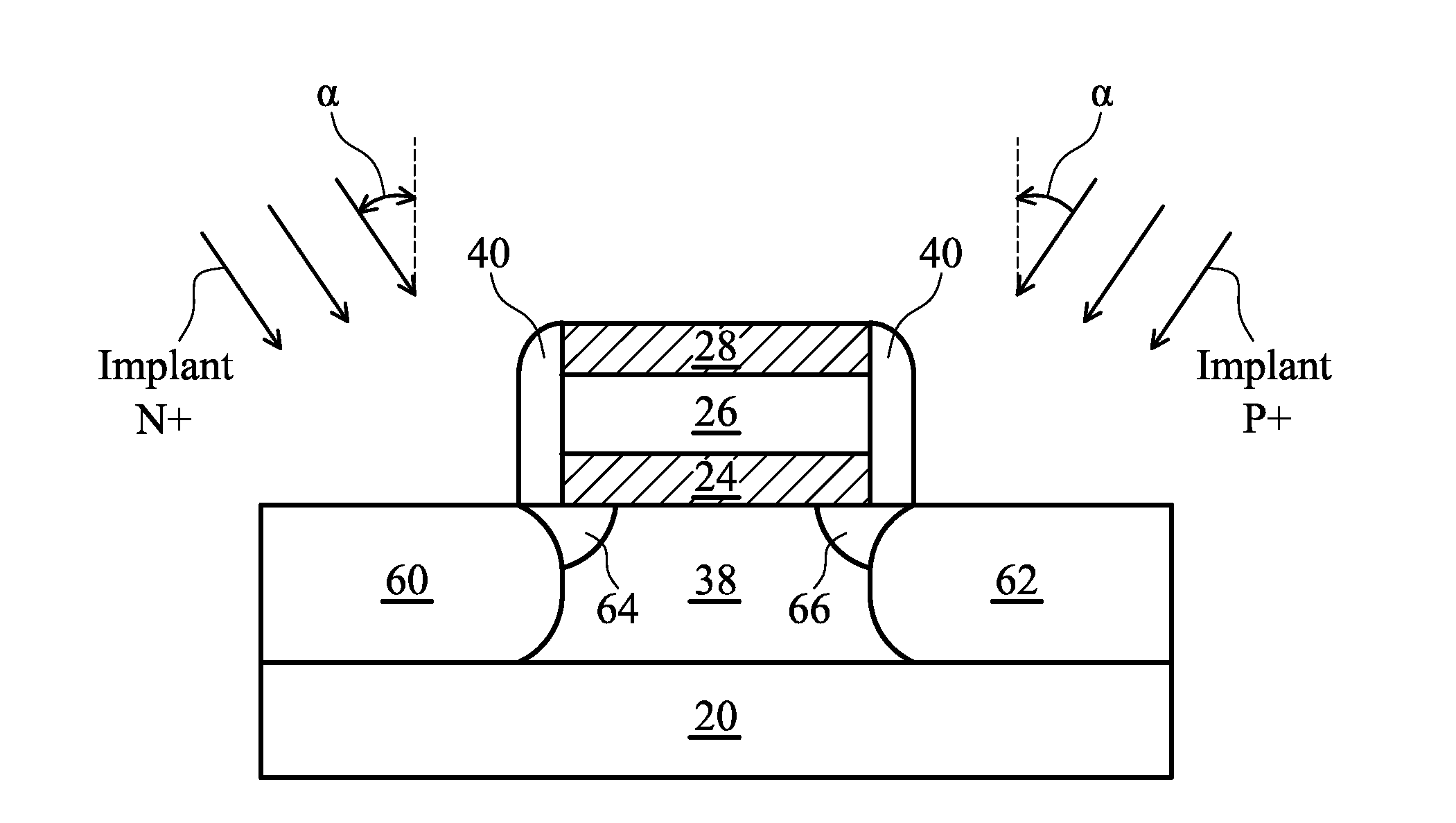
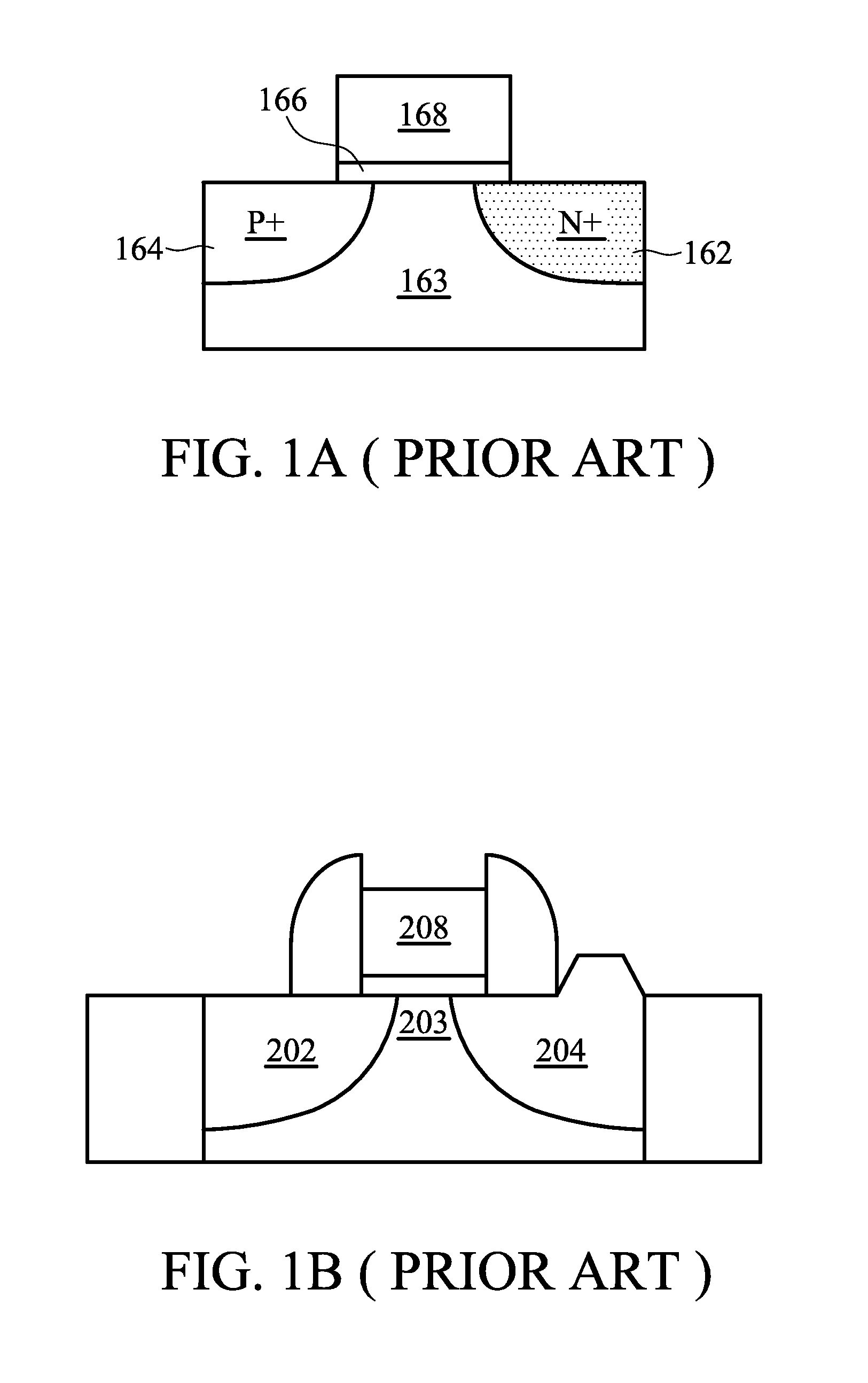
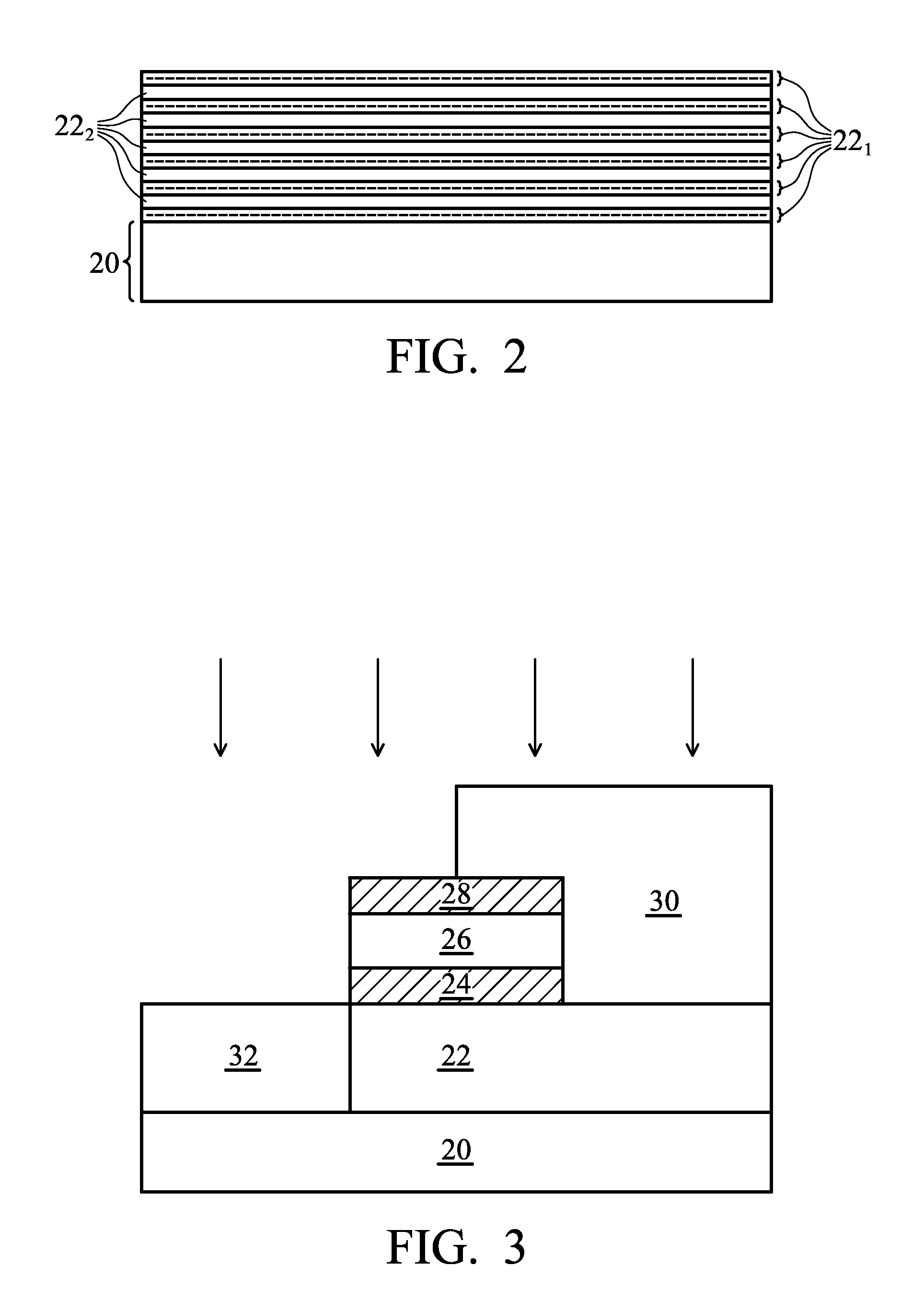
[0028]A first embodiment of the present invention is provided in FIGS. 2 through 9. Referring to FIG. 2, substrate 2...


PUM


Abstract

A semiconductor device includes a channel region; a gate dielectric over the channel region; a gate electrode over the gate dielectric; and a first source / drain region adjacent the gate dielectric. The first source / drain region is of a first conductivity type. At least one of the channel region and the first source / drain region includes a superlattice structure. The semiconductor device further includes a second source / drain region on an opposite side of the channel region than the first source / drain region. The second source / drain region is of a second conductivity type opposite the first conductivity type. At most, one of the first source / drain region and the second source / drain region comprises an additional superlattice structure.

Description

CROSS-REFERENCE TO RELATED APPLICATION[0001]This application relates to commonly assigned U.S. patent application Ser. No. 11 / 828,211, filed Jul. 25, 2007, and entitled “Tunnel Field-Effect Transistor with Narrow Band-Gap Channel and Strong Gate Coupling” which application is hereby incorporated herein by reference.TECHNICAL FIELD[0002]This invention relates generally to semiconductor devices, and more specifically to tunnel field-effect transistors (FETs) having superlattice channels.BACKGROUND[0003]Metal-oxide-semiconductor (MOS) is a dominating technology for integrated circuits at 90 nm technology and beyond. A MOS device can work in three regions, depending on gate voltage Vg and source-drain voltage Vds, linear, saturation, and sub-threshold regions. The sub-threshold region is a region where the gate voltage Vg is smaller than the threshold voltage Vt. The sub-threshold swing represents the easiness of switching the transistor current off and thus is an important factor in de...

Claims


Application Information

Patent Timeline
Patent Type & Authority Patents(United States)
IPC IPC(8): H01L29/94
CPCH01L21/26586H01L29/66545H01L29/66636H01L29/66659H01L29/7835H01L29/7391
Inventor BHUWALKA, KRISHNA KUMARWANG, CHING-YAGOTO, KEN-ICHILEE, WEN-CHINDIAZ, CARLOS H.
Owner TAIWAN SEMICON MFG CO LTD
Why Eureka
Try Eureka