Nanowire structures comprising carbon
a technology of nanowires and carbon, which is applied in the manufacture of cell components, final product manufacturing, electrochemical generators, etc., can solve the problems of large quantity of expensive platinum (and/or ruthenium) catalysts, low efficiency and power density, and inability to embrace dmfcs, etc., to achieve high electrical connectivity, low overall diffusion resistance, and high structural stability
- Summary
- Abstract
- Description
- Claims
- Application Information
AI Technical Summary
Benefits of technology
Problems solved by technology
Method used
Image
Examples
example 1
Preparation of Nanowire Structures
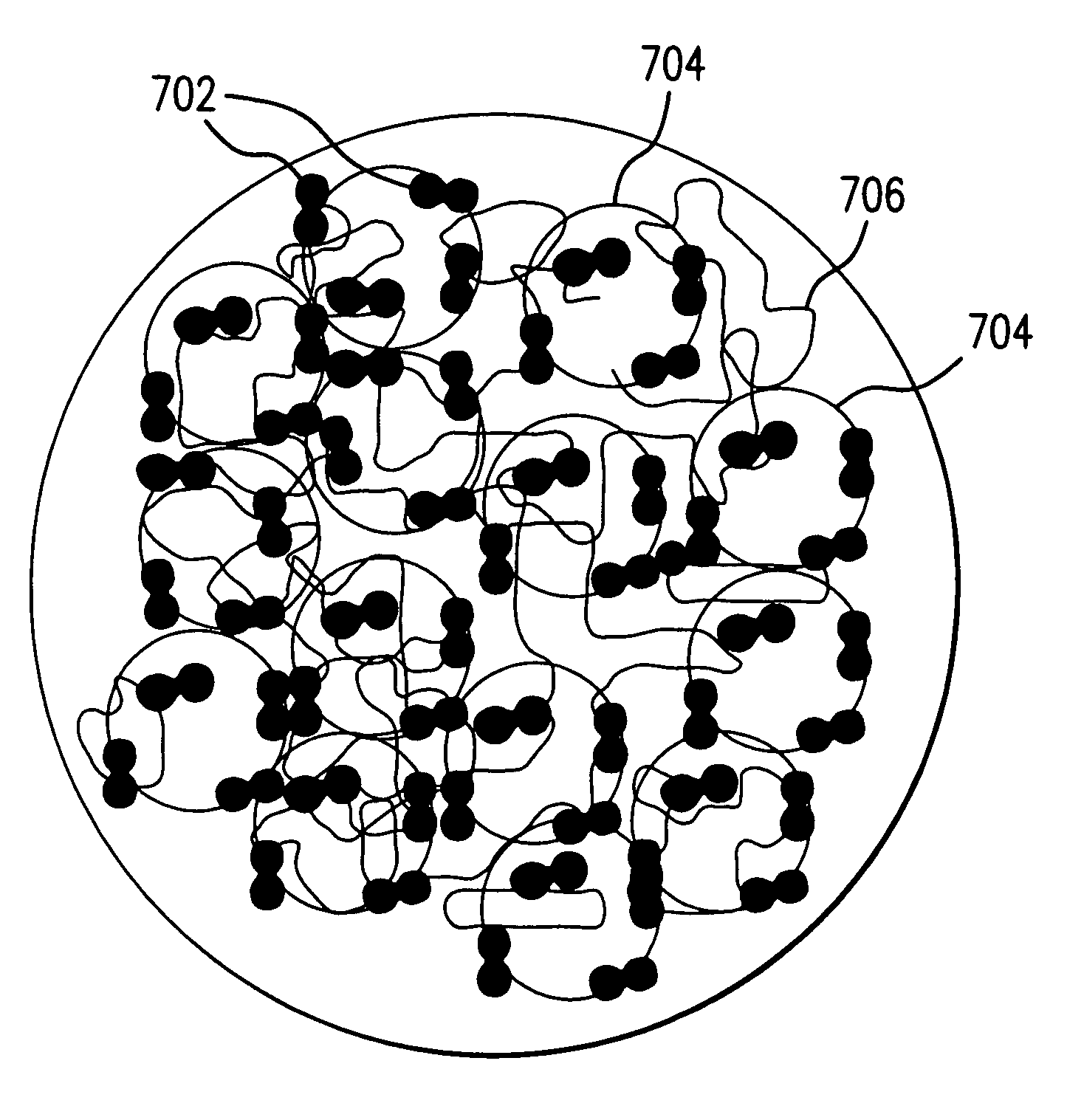
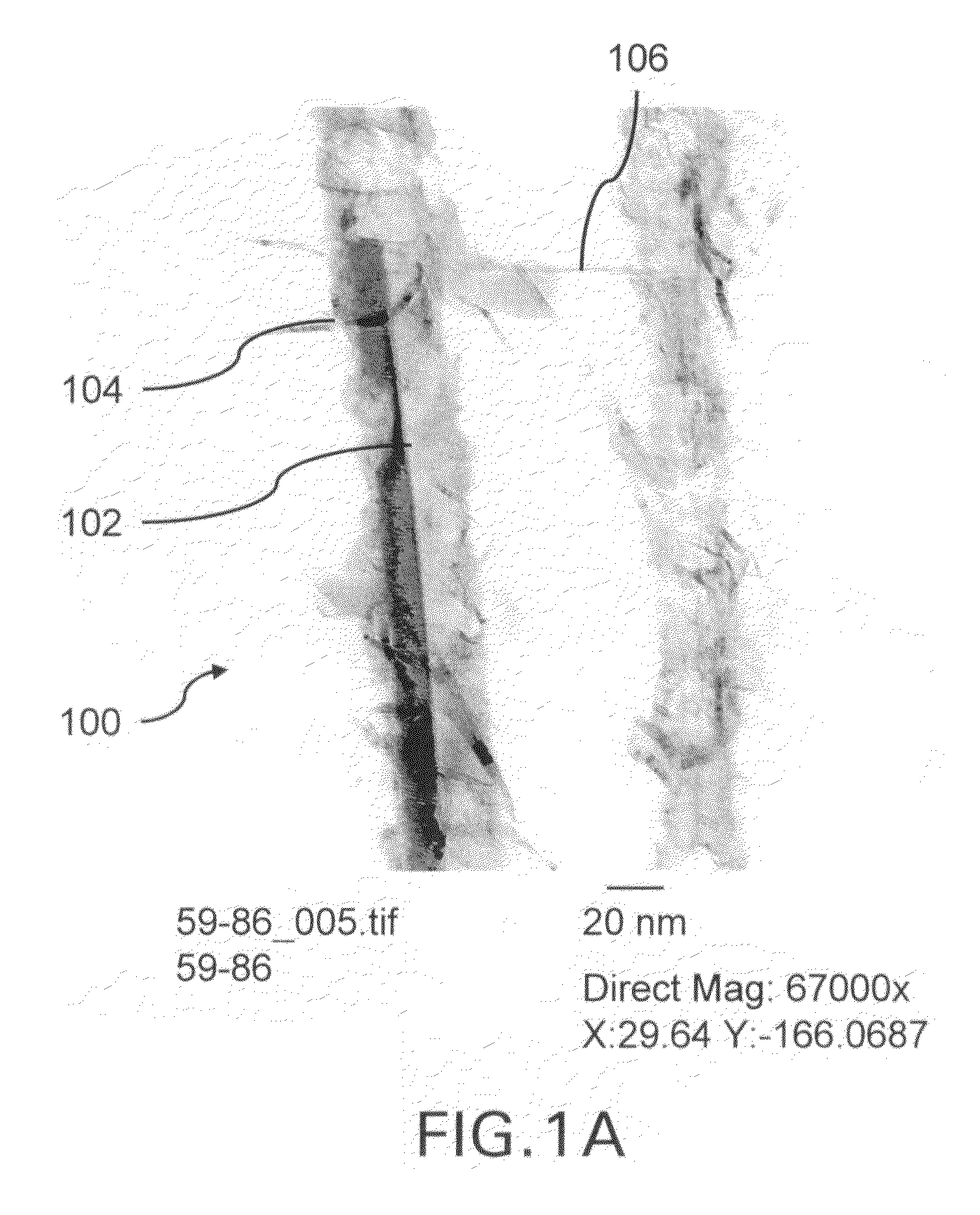
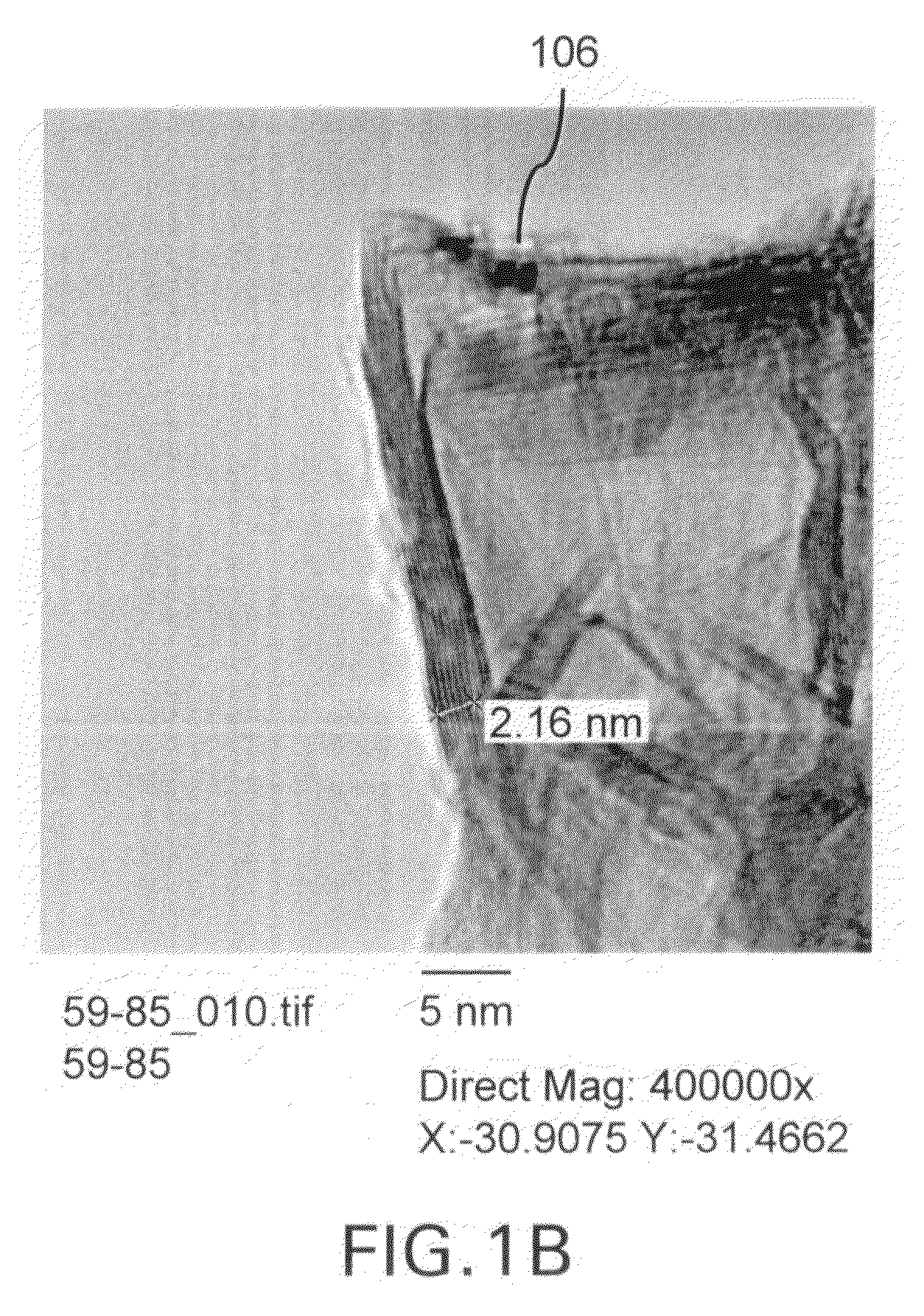
[0252]Silicon nanowires coated with WO3 were heated at 650° C. for 30 minutes, followed by 1250° C. for 6 min in the presence of a flowing gas mixture comprising Ar (430 cc / min), H2 (130 cc / min) and CH4 in Ar (228 cc / min). After the preparation was cooled, an interconnected nanowire network 300 comprising interconnected nanowire structures 100 was formed. The nanowire structures 100 comprising Si nanowire cores 102, carbon based layers 104 (SiC / WC interfacial carbide layers) and carbon-based structures 106 (graphene nanographitic plates) connecting the nanowire structures 100.
example 2
Deposition of Nanoparticles on Nanowires
[0253]Approximately 10 mg Si nanowires were dispersed in ethanol by sonication to form a nanowire suspension. An interconnected nanowire network was prepared by vacuum filtration of the nanowire suspension over a polyvinylidene fluoride (PVDF) membrane and vacuum drying, then 2 cc 0.1% polylysine solution was added to the filter funnel to absorb polylysine on the surface of the nanowires. After 5 minutes, all liquid in the funnel was vacuum removed and the nanowire network was separated from the PVDF membrane. After being dried in an oven at 100® Celsius for 15 minutes, the nanowire network was submerged in 10 cc of Au colloid solution (10 nm colloids) and soaked for 20 minutes to absorb the Au nanoparticles on the surface of the nanowires. Finally, the nanowire network was removed from the Au colloid solution, rinsed with isopropyl alcohol (IPA), and dried at 100° Celsius to obtain a nanowire network coated with gold nanoparticles. FIG. 14 sh...
example 3
Fabrication of Densely Packed Nanowires
[0254]In order to examine methods to increase packing density of nanowires, “bird's-nest'” structures of 60 nm silicon nanowires were prepared using various techniques. The results of the methods are represented below in Table 1:
[0255]
TABLE 1MethodPacking Density Relative to Silicon DensityAs collected on the filter6%Stirred with shear mixer6.1%Uniaxially pressed11.2%Surfactant (Triton X-100)8%Die pressed, 40 KPSI46.6%Compact Packing (90°)78.5%Compact Packing (0°)90.7%
[0256]The packing density prepared by filtering the dispersion of 60 nm nanowires was 6%. Stirring the dispersion with a high speed shear mixer prior to filtration did not improve the packing density. A packing density increase of more than 30% was noted by adding surfactant (Triton X-100) to the nanowire dispersion prior to filtration. A significant increase in packing density was observed after application of uniaxial pressure to the nanowires. A packing density of 46.6% was mea...
PUM
| Property | Measurement | Unit |
|---|---|---|
| angle | aaaaa | aaaaa |
| angle | aaaaa | aaaaa |
| distance | aaaaa | aaaaa |
Abstract
Description
Claims
Application Information


