Method and apparatus for substrate noise aware floor planning for integrated circuit design

a technology of integrated circuit design and floor plan, applied in cad circuit design, program control, instruments, etc., can solve the problems of noise injection to the substrate, noise handling, signal integrity issues that are increasingly becoming more critical, etc., and achieve the effect of reducing the impact of switching nois

Active Publication Date: 2011-01-04
CADENCE DESIGN SYST INC
View PDF19 Cites 32 Cited by
  • Summary
  • Abstract
  • Description
  • Claims
  • Application Information

AI Technical Summary

Benefits of technology

[0020]Thus, a methodology is provided to perform noise analysis early in the design of an integrated circuit, such as a mixed signal IC. Based upon analysis re

Problems solved by technology

Furthermore, in the deep submicron regime signal integrity issues are increasingly becoming more critical.
One of the most significant signal integrity problems in mixed signal designs today is the handling of noise coupled through the common substrate caused by power supply fluctuations due to simultaneous switching of digital cells.
The main sources of noise injection to the substrate are noise due to digital switching including noise on the ground contacts and on VDD contacts due to switching transients.
Substrate noise can result in un-intended interaction between the digital and analog components of a chip through the underlying silicon substrate.
Analog systems generally lack the degree of noise immunity of digital circuits, and the substrate coupling noise can degrade analog performance.
Substrate noise can cause fluctuations in the voltage potential of the substrate, which can affect CMOS device behavior.
For a digital circuit, this could result in a small change in the delay of a logic gate.
However, for an analog circuit, the effect can be much more severe.
For instance, in an amplifier, a change in threshold voltage can change the operating point of the amplifier and significantly reduce the gain.
Digital circuit switching generates substrate noise through multiple mechanisms.
For instance, digital circuit switchin

Method used


Image

  • Method and apparatus for substrate noise aware floor planning for integrated circuit design
  • Method and apparatus for substrate noise aware floor planning for integrated circuit design
  • Method and apparatus for substrate noise aware floor planning for integrated circuit design

Examples


Embodiment Construction

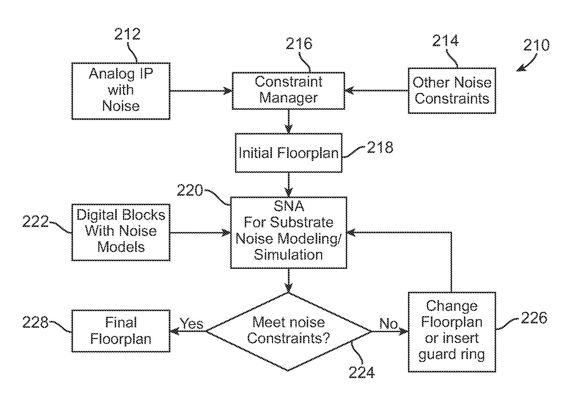
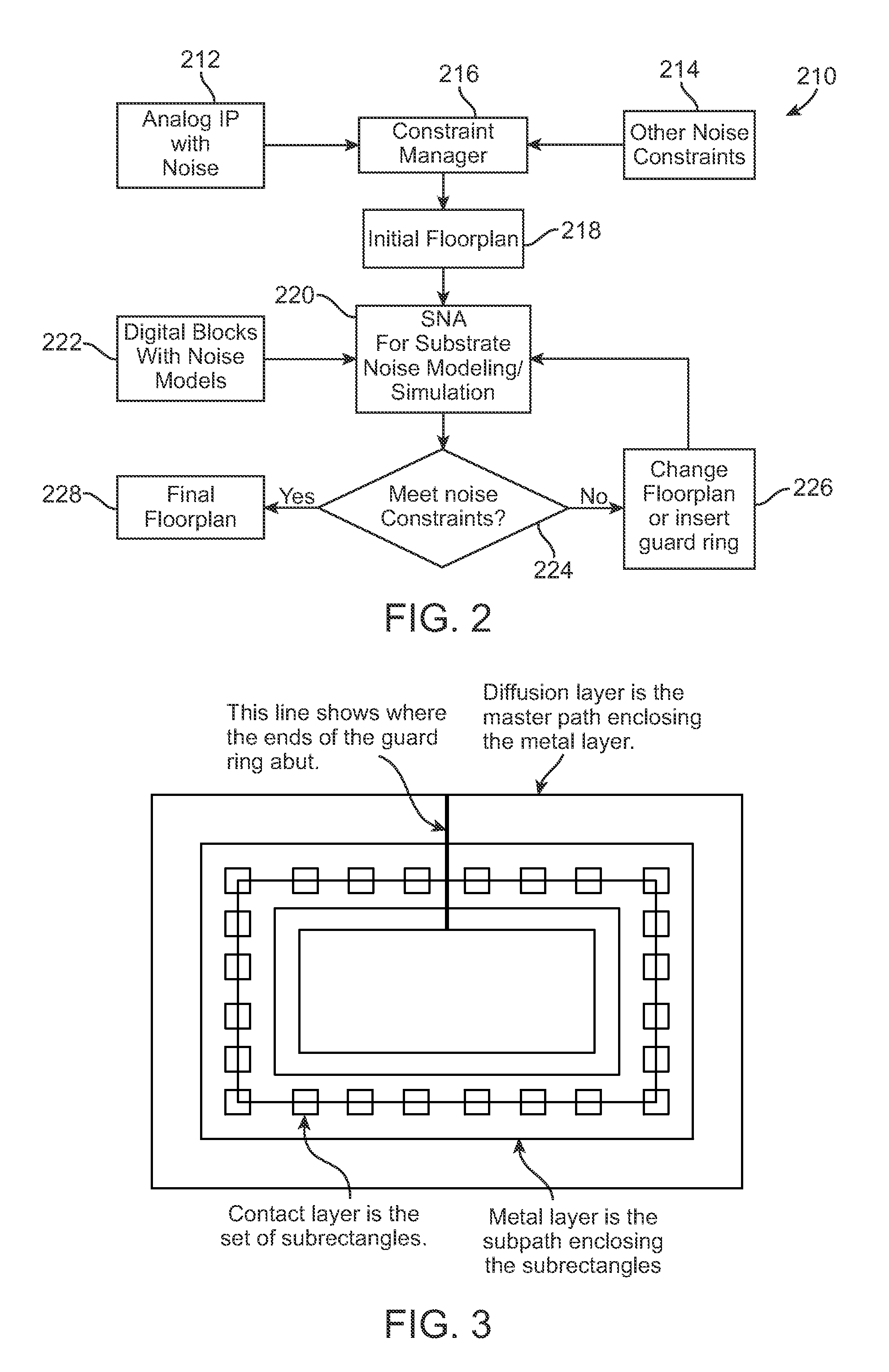
[0035]The following description is presented to enable any person skilled in the art to make and use a computer implemented system and method and apparatus to use substrate noise information in the development of a floorplan early in an integrated circuit design flow in accordance with embodiments of the invention, and is provided in the context of particular applications and their requirements. Various modifications to the preferred embodiments will be readily apparent to those skilled in the art, and the generic principles defined herein may be applied to other embodiments and applications without departing from the spirit and scope of the invention. Moreover, in the following description, numerous details are set forth for the purpose of explanation. However, one of ordinary skill in the art will realize that the invention might be practiced without the use of these specific details. In other instances, well-known structures and processes are shown in block diagram form in order ...


PUM


Abstract

A methodology is provided to perform noise analysis in the implementation stage of the design of an integrated circuit, and based upon analysis results, a floorplan may be adjusted or guard rings may be inserted to reduce the impact of digital switching noise upon noise sensitive circuits.

Description

CROSS REFERENCE TO RELATED APPLICATION[0001]The subject matter of this application claims priority to commonly-owned U.S. Provisional Patent Application Ser. No. 60 / 892,204 entitled DIGITAL BLOCK MODELING AND METHOD AND APPARATUS FOR SUBSTRATE NOISE AWARE FLOOR PLANNING FOR MIXED SIGNAL SOCs, filed on Feb. 28, 2007, which is expressly incorporated herein by this reference.BACKGROUND OF THE INVENTION[0002]1. Field of the Invention[0003]The invention relates in general to floorplanning during design of integrated circuits and more particularly, to use of estimated substrate noise as a constraint during floorplanning.[0004]2. Description of the Related Art[0005]With the increasing levels of integration in chip design, more SOCs are being developed that have digital, analog and RF functions integrated on a single chip substrate. Furthermore, in the deep submicron regime signal integrity issues are increasingly becoming more critical. One of the most significant signal integrity problems...

Claims


Application Information

Patent Timeline
IPC IPC(8): G06F17/50
CPCG06F17/5036G06F17/5068G06F30/367G06F30/39
Inventor KAO, WILLIAMDONG, XIAOPENG
Owner CADENCE DESIGN SYST INC
Why Eureka
Try Eureka