Heat spreading circuit assembly

a circuit assembly and heat spreading technology, applied in the field of circuit assembly, can solve the problems of high cost of thermally conductive particles, large amount of heat that print circuit boards must help dissipate, and large amount of heat generated by components that must be dissipated, and achieve the effect of improving heat spreading capabilities

Inactive Publication Date: 2011-02-15
NEOGRAF SOLUTIONS LLC
View PDF53 Cites 50 Cited by
  • Summary
  • Abstract
  • Description
  • Claims
  • Application Information

AI Technical Summary

Benefits of technology

[0023]It is an object of the invention to provide a c...

Problems solved by technology

Such components can generate substantial amounts of heat that must be dissipated for them to operate reliably and to their intended performance levels
As a result of these heat generating components, the amount of heat that print circuit boards must help dissipate can be significant.
The use of thermally conductive particles can be expensive, however, and the subsequent layer must be thick enough to ensure it is pin-hole free, adding to thermal resistance in the design.
Additional limitations of this approach arise from the lack of flexibility to fabricate bent or non-planar circuit structures, and the fact that the dielectric material covers the entire surface of the heat spreader layer.
The use of anodization as the dielectric layer attempts to overcome some of these issues, but forces the use of aluminum as its heat spreader layer, since copper cannot be anodized.
Since the thermal conductivity of aluminum is significantly less than that of copper, this can be a thermal disadvantage.
All of the foregoing approaches, however, can suffer soldering difficulties, since the same heat dissipation properties that are useful during the operation of the printed circuit board and components, inhibit an assembly process that requires point sources of heat for soldering (such as hot bar bonding, for example).
Moreover, traditional heat spreading materials like copper or aluminum also add significant weight to the board, which is undesirable, and the coefficient of thermal expansion (CTE) of these materials may not closely match that of the glass fiber laminate, leading to physical stress on the printed circuit board with the application o...

Method used


Image

  • Heat spreading circuit assembly
  • Heat spreading circuit assembly
  • Heat spreading circuit assembly

Examples


Embodiment Construction

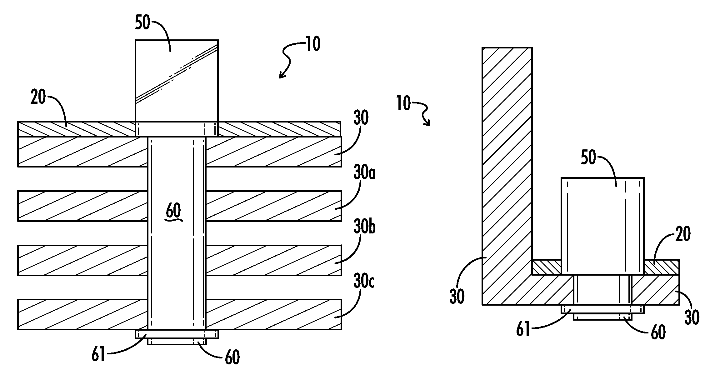
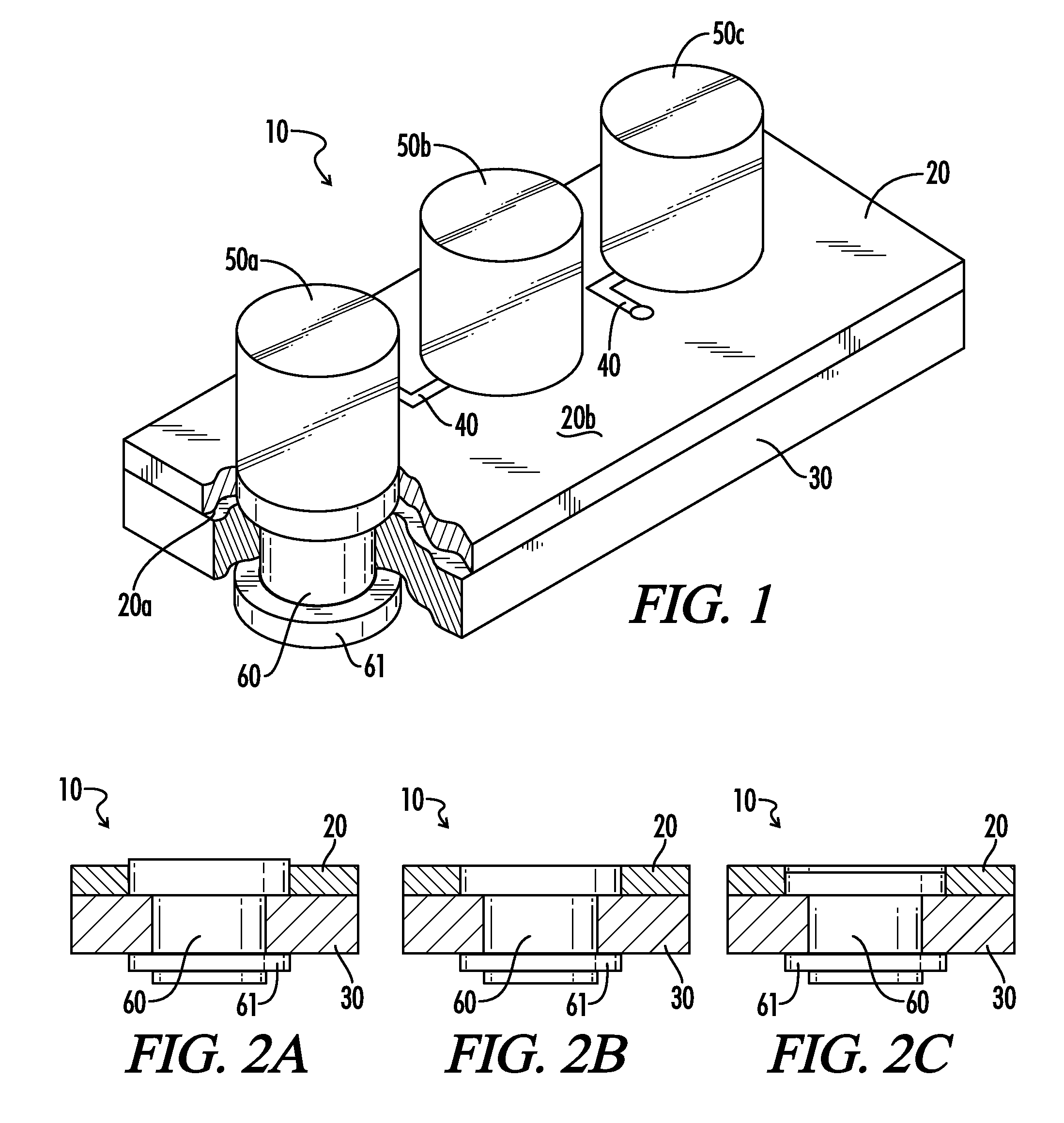
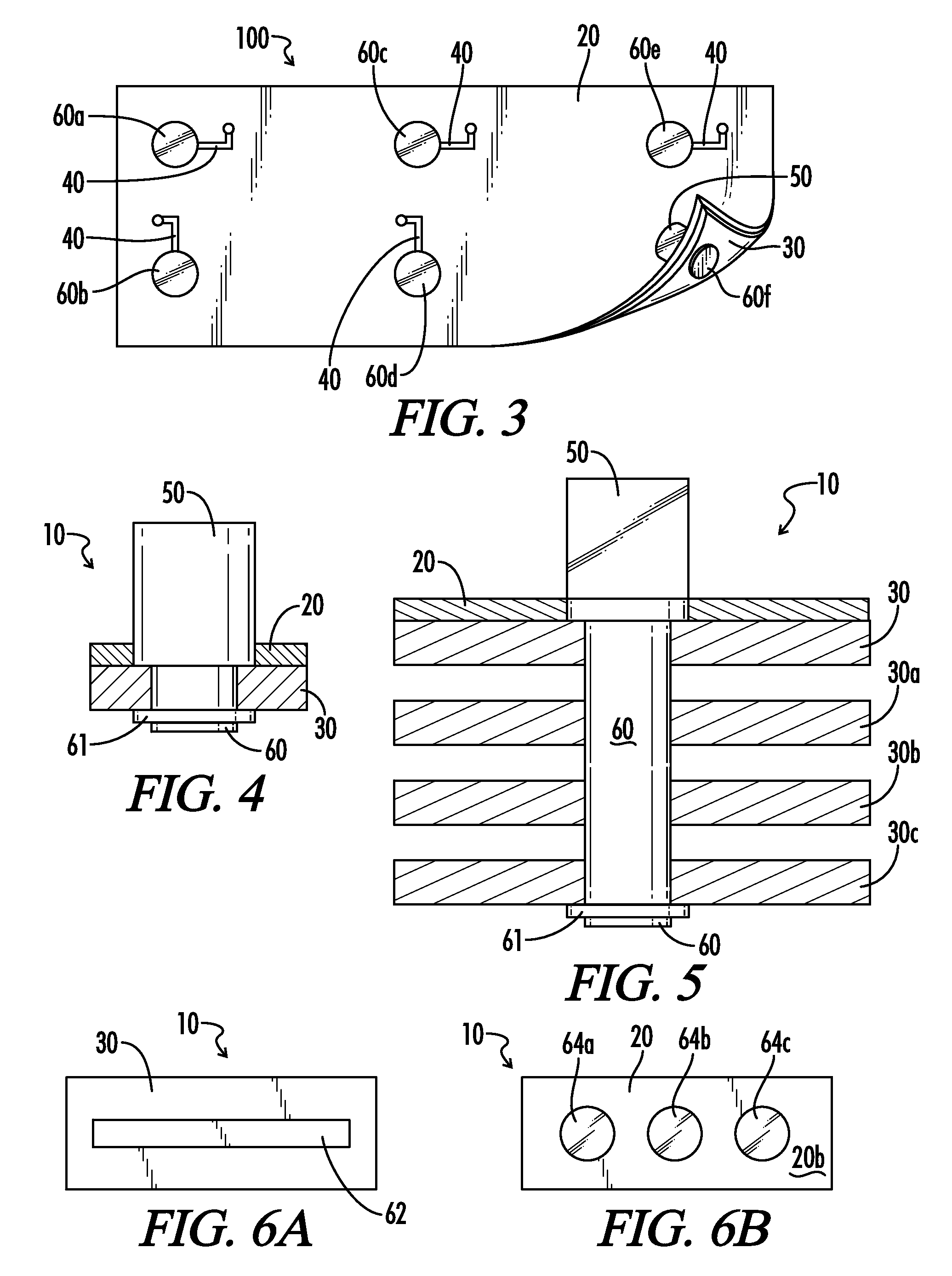
[0037]This invention is based upon the finding that the heat spreading function of a heat spreader layer on a circuit assembly is substantially improved when a thermal pathway between a heat-generating component, especially an LED, and the heat spreader layer is provided. Indeed, by the use of such a thermal pathway, the use of graphite-based heat spreader layers can provide improved heat spreading, even as compared to the use of aluminum or copper heat spreaders, with the added benefit of reduced weight.

[0038]By the term “circuit assembly” is meant an assembly including one or more electronic circuits positioned on a dielectric material, and can include laminates where one or more of the circuits is sandwiched between layers of dielectric material. Specific examples of circuit assemblies are printed circuit boards and flex circuits, as would be familiar to the skilled artisan.

[0039]Before describing the manner in which the invention improves current materials, a brief description o...


PUM

PropertyMeasurementUnit
Angleaaaaaaaaaa
Lengthaaaaaaaaaa
Thicknessaaaaaaaaaa

Abstract

A circuit assembly including a substrate which has a dielectric layer, a heat spreader layer located at a first surface of the substrate, a heat generating component located at a second surface of the substrate, and a thermal pathway in thermal connection between the heat spreader layer and the heat generating component.

Description

TECHNICAL FIELD[0001]The present invention relates to a circuit assembly having improved heat spreading capabilities. The inventive circuit assembly includes a heat source, such as a light emitting diode (LED) disposed on a circuit assembly substrate, a heat spreader layer disposed on the circuit assembly substrate and a thermal pathway between the heat generating component and the heat spreader layer.BACKGROUND OF THE INVENTION[0002]Printed circuit boards are conventionally manufactured from dielectric materials such as glass fiber laminates (known as FR4 boards), polytetrafluoroethylene, and like materials. On one of the surfaces of such boards, or between layers of dielectric materials, are circuits, usually formed of copper. The circuits are commonly formed by photolithographic methods, sputtering, screen printing or the like (for circuits disposed between layers, the circuit is applied to the dielectric material before formation of the laminate). In addition, components such as...

Claims


Application Information

Patent Timeline
IPC IPC(8): H05K7/20
CPCH05K1/0203H05K7/205H05K1/182Y10T428/24802H01L2924/0002H05K2201/10106H01L2924/00
Inventor REIS, BRADLEY E.CARTIGLIA, JAMES R.
Owner NEOGRAF SOLUTIONS LLC
Why Eureka
Try Eureka